Layer-by-layer fabrication has long been used for industrial prototyping, but a boom in lower-cost, desktop 3D printers is broadening its appeal and materials suppliers are responding as markets for these versatile tools expand.
Polymer pellets. Image credit: Arkema.
This week, Arkema – whose company history goes back to a reorganization of Total’s intermediate chemicals group in 2004 – announced that it is adding 3D printing as a 6th ‘innovation driver’ for its international research and development (R&D) operation. ‘Materials for 3D printing’ joins existing R&D programmes in ‘lighter materials’, ‘renewable raw materials’, ‘materials for energy’, ‘water treatment solutions’ and ‘materials for electronics’.
Arkema offers polymers for laser sintering as well as UV-curable resins, and is developing formulations that can be used to make extremely tough 3D-printed products. But it’s not just the big firms that are busy innovating and ramping up the range of materials available to the growing 3D printing community. Materials start-ups and university labs are also participating in the translation of novel feedstock.
The Flextech Alliance has created a map (JPEG format) of its 150+ partner network, which clusters around nano-bio; flex substrates; design, modelling and testing; equipment and materials; deposition and printing; CMOS thinning; packaging; and standards.
According to the announcement, the funding, which runs for five years, will be matched by more than $96 million in cost sharing from non-federal sources, including the City of San Jose, private companies, universities, several U.S. states, and not-for-profit organizations.
Beyond defence applications, other markets for flexible hybrid electronics include automotive, communications, consumer electronics, medical devices, health care, transportation and logistics, and agriculture.
Nanotechnology
SEP 2015 – the US National Science Foundation (NSF) is providing $81 million over five years to support 16 sites and a coordinating office as part of a new National Nanotechnology Coordinated Infrastructure (NNCI).
The NNCI framework is the successor to the National Nanotechnology Infrastructure Network (NNIN), which – as the program synopsis outlines – provided researchers from academia, small and large companies, and government with open access to university user facilities with leading-edge fabrication and characterization tools, instrumentation, and expertise within all disciplines of nanoscale science, engineering, and technology.
Advanced materials translation
SEP 2015 – Designing Materials to Revolutionize and Engineer our Future (DMREF) is the NSF’s ‘primary program’ for participating in the Materials Genome Initiative – a multi-agency initiative to accelerate advanced materials discovery and deployment by exploiting advances in computational techniques, and making more effective use of standards, and enhanced data management.
Recognizing the multi-disciplinary nature of the task, DMREF reaches across various NSF directorates including Mathematical and Physical Sciences; Engineering; and Computer and Information Science and Engineering.
DMREF funding consists of 20 – 25 grants of between $750,000 and $1,600,000 to develop, for example, new data analytic tools and statistical algorithms; advanced simulations of material properties in conjunction with new device functionality; advances in predictive modeling that leverage machine learning and data mining; and new collaborative capabilities for managing large, complex, heterogeneous and distributed data.
Eurekite, an advanced materials spin-off from the University of Twente in the Netherlands that refers to its non-brittle, nanofibre-based products as ‘flexiramics’, has attracted a EURO 1 million investment from Cottonwood – a US venture capital (VC) firm with a European hub in Twente’s largest city, Enschede. The university start-up plans to use the VC funding to deliver prototypes based on its 100% ceramic materials, which were first developed at the MESA+ Institute of Nanotechnology, and to scale-up its operation.
Designer material: flexible 100% ceramic developed at MESA+ and available via Eurekite – a spin-off from the University of Twente. Image credit: Eurekite
“We have created a material that merges the properties of paper and ceramics,” says Eurekite co-founder Bahruz Mammadov (COO/CFO) who formed the company less than a year ago together with Gerard Cadafalch (CEO). Andre ten Elshof, a senior faculty member at MESA+, joins them as chief scientific officer. The team has strong connections to research programmes at the University of Twente investigating the properties of electrospun ceramic nanofibers. Based on promising results in the lab, the team decided to explore commercial opportunities for these tough and flexible nanomaterials.
Like conventional ceramics, Eurekite’s products don’t burn, but as the name suggests ‘flexiramics’ are much less fragile than traditional formulations and don’t shatter when dropped. The team hopes that this rugged combination of properties will inspire designers, and potential applications include high-temperature oil & gas sensors, flexible substrates for mobile phone antennas, lithium-ion battery energy performance upgrades, high-power electronics for electric vehicles and solar energy – to name just a few uses for ‘flexiramics’!
Ecosystem built for translation
As TMR+ witnessed on a tour of the region back in 2013, the University of Twente offers a healthy ecosystem for translating materials research from the laboratory through to the market. In addition to MESA+, local facilities include a prototyping environment (NanoLab) and the nearby High Tech Factory where early-stage companies can ramp-up to higher production volumes.
Semiconducting polymers are a key ingredient in organic light emitting diodes (OLEDs), organic photovoltaics (OPVs) and organic field effect transistors (OFETs) – and pave the way for future bendable electronic devices. The technology is driving advances in the design of flexible displays, conformable energy harvesters, and wearable sensors to name just a few applications. What’s more, thanks to their solubility in many organic solvents, semiconducting polymers provide device makers with a range of appealing fabrication options including ink-jet printing, spray-coating and roll-to-roll production.
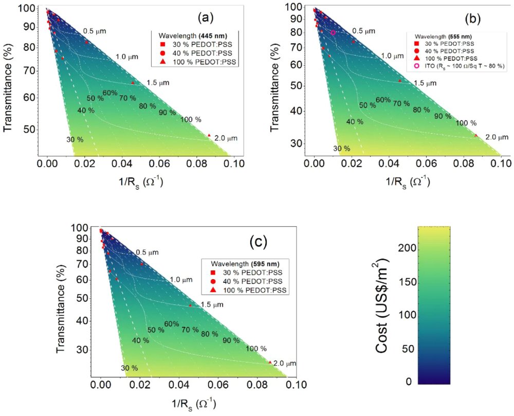
Graphical guidelines: a series of figure of merit charts show the interplay between key performance parameters for different blends and film thicknesses of PEDOT:PSS/PVA (Olivia Carr et al 2015 Transl. Mater. Res. 2 015002).
Optimizing the composition of the blended film is important to balance the cost versus performance. In many cases, high electrical conductivity and high optical transmittance in the visible range of the electromagnetic spectrum are critical factors. However, other aspects such as flexibility, film formation, chemical stability and wettability can also play an important role in the choice of the material or the composition to be used, together with overall processing considerations.
Case study: semi-transparent electrodes for flexible optoelectronics
In a recent study, published in the journal Translational Materials Research (TMR), materials scientists have examined a blend comprising poly(3,4-ethylenedioxythiophene):polystyrene sulfonate (PEDOT:PSS) and polyvinyl alcohol (PVA), which can be used as a flexible, semi-transparent and highly-conductive material in electronic and optoelectronic devices. The electrical conductivity and optical transmittance of spray-deposited films of various thicknesses and blend ratios were evaluated to determine the most appropriate composition for optimal device performance and cost.
Presenting their results as a series of figure of merit diagrams, the researchers observe that it should be possible to decrease the PEDOT:PSS content in the blend down to 30% (by weight) and maintain an acceptable level of electrical conductivity for many applications.
Angstron Materials, a US supplier of single and few-layer graphene materials, announced this week that it has secured $5 million in capital to increase manufacturing capacity and bring key technologies such as its thermal management products to market. Heat spreaders developed by the firm can reduce hot-spots in mobile phones and other handheld devices, and the funding news follows reports earlier this year that Angstron’s graphene sheets have been qualified for use by a major mobile electronics company.
Thermal interface material: Angstron Materials supplies graphene-based sheets in thicknesses ranging from 5 µm to 40 µm with thermal conductivity between 800 W/m.K and 1700 W/m.K for use in electronic products such as tablets, laptops and flat screen TVs. The foils can also be used for EMI shielding.
Estimates by market analyst IDTechEx suggest that 55% of electronic failures are caused by over-heating, and enhanced thermal interface materials have a major role to play in helping devices to stay cool, perform better and last longer as developers boost their offerings by packing more processing power into increasingly compact form-factors.
“We use the planar alignment of carbon atoms to make a lightweight, flexible thermal foil with up to 1700 W/m.K in-plane thermal conductivity – substantially higher thermal conductivity than copper and offering weight savings for thermal management,” Claire Rutiser, a member of Angstron’s executive team, told TMR+. “Also, we can load thermally conductive nano graphene platelets (NGP) into a matrix – which could be thermoset, thermoplastic or non-curing (for thermal paste).”
Graphene isn’t the only option for device makers and competing thermal management materials include formulations based on silver flakes or silver nano-wires, but there are economic considerations that may favour the use of NGPs. “Silver is subject to significant price fluctuation and future price uncertainty,” Rutiser comments. “Angstron Materials has known input materials pricing and is able to enter into long term supply agreements with end users.”
Graphene has been linked with various big names in portable electronics. In 2011, Apple noted that the use of graphene thermal dissipators goes beyond cooling. Related applications include transferring heat from onboard electronics to the battery to improve runtime, which can be compromised at low temperatures.
Multiple markets
Rutiser says that Angstron is ready with scalable production capacity and emphasised that the firm is targeting other sectors in addition to thermal management materials. She’s optimistic that over a 10 year period energy storage will grow to become one of the company’s biggest sources of revenue. Driving this are developments in graphene-wrapped silicon anodes by sister company Nanotek Instruments, which allow fabrication of Li-ion batteries with over 400 Wh/kg, and also materials for supercapacitors.
“Affordable, high-capacity energy storage is critical for the transition to electric vehicles and for grid-stabilization as the percentage of energy derived from renewables increases in the coming decades,” Rutiser explained. “These products have comparatively long qualification times due to reliability testing and industry safety standards.”
Currently, Angstron’s graphene-enhanced products and technologies are linked to five distinct portfolios – thermal management materials, energy storage systems, nanocomposites, transparent conductive films, paints and coatings. “Graphene platelets are inert to most chemical species and offer opportunities to improve barrier coatings against corrosion, chemical attack, or oxygen permeation, “ added Rutiser.
In its latest report on emerging technologies, Lux Research has put the spotlight on opportunities for smart coatings. The firm’s analysis highlights the power of partnerships in translating breakthroughs from the lab to the market, which has implications for start-ups in the field of advanced materials. To find out more, TMR+ spoke with Anthony Schiavo, an analyst at Lux Research and lead author of Surfaces Get Smarter: Scouting Emerging Coatings, Markets and Functionalities.
New roles beyond protection
“Today, coatings can do more than just provide protection,” said Schiavo. “They are finding new roles and replacing other components such as inspection systems.” Examples can be found in the US Navy, which has patented a resin that releases a distinct odour when broken. This feature can be exploited to alert crew members to corrosion and mechanical fatigue in out of sight areas of a ship or aircraft.
The Navy system has been designed with the human nose in mind, but there are automated solutions out there too. Another approach involves coating RFID tags with a conductive layer. “When the coating is damaged, the signal will propagate,” explained Schiavo.
Smart materials as a service
The oil and gas sector is another strong prospect for smart coatings, but as Schiavo points out – performance is only part of the picture. Materials suppliers need to pick the right revenue model to ramp up their business.
“Solutions will be more attractive to potential customers if providers can supply advanced materials and coatings as a service rather than a product,” he said. “Suppliers can lower the barrier to entry by tying the value of their products directly to performance, in this case an improvement in downtime figures, rather than attempting to sell tonnes of material outright in advance.”
Cost-benefit analysis
Winners in the consumer electronics segment include firms such as P2i, a provider of chemically bonded hydrophobic coatings, which allow device partners to add-value in highly competitive sectors such as the mobile phone market. “The differentiation you get on a raw technology basis can be very short-lived,” commented Schiavo. “Smart coatings help manufacturers to strengthen the appeal of their products.”
Other exciting firms to watch include LiquiGlide and SLIPS Technologies, which are positioned to impact packaging. Like P2i, their value proposition can be communicated in just a few seconds of video or by a quick product demo, which makes it much easier for these companies to pitch their technology to potential partners.
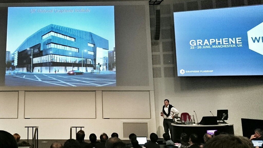
The UK welcomed an influx of graphene experts last week as Manchester University’s 200+ researchers working in the field of 2D materials were joined by hundreds more for Graphene Week 2015. The event, now in its 10th year, has grown from a small European workshop into a five-day conference boasting over 600 attendees and pushing the University Place venue to capacity. The scope of the programme has expanded too; hexagonal boron nitride (hBN), molybdenum disulphide (MoS2) and other related 2D materials have joined graphene on the ‘menu’ of structures being explored by developers. Most recently, the conference has been co-ordinated by the Graphene Flagship – a European drive to capitalize on the many opportunities for 2D materials, which launched in October 2013 and has adopted Graphene Week as its annual conference.
Plenary update: Nobel Prize winner Kostya Novoselov briefed the Graphene Week 2015 audience on major developments in the field of 2D materials.
The European Commission (EC) has given graphene and related 2D materials research a huge boost through its Flagship initiative, but as Thomas Skordas, head of the EC’s FET Flagships Unit, reminded the audience during the conference opening – the funding is not a blank cheque for 10 years. The objective is to deliver economic benefits. So far, Graphene Flagship projects have generated 3x more publications compared with the Horizon 2020 average, but to achieve its long term goal the programme needs to capitalize on this research growth.
Connecting with industry
The challenge of taking graphene and related 2D materials from the lab to the market is a focus issue for TMR+ and its sister journal Translational Materials Research (TMR), and we were delighted to be invited to the Flagship’s latest Graphene Connect workshop, co-located with Graphene Week 2015, to join in the discussion.
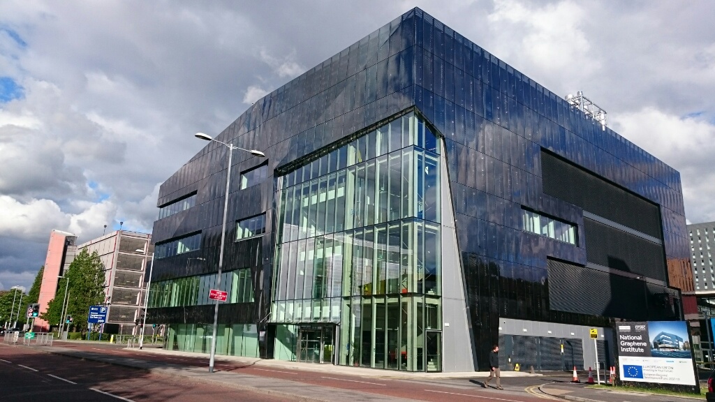
New facility: the Graphene Connect networking event focusing on investment opportunities was held at the UK’s National Graphene Institute in Manchester.
The Manchester session was focused on investment opportunities in graphene and related 2D materials, and put the spotlight on start-ups and early-stage companies. Fittingly, the workshop took place at the recently opened National Graphene Institute (NGI) – a facility where academia and industry are co-located to promote translation of 2D materials from the lab to the market.
Presenters from the VC community included Achim Hoffman of IP Group. He picked up on the issue of media hype surrounding graphene, which has distorted expectations. One of the key messages from the session was the need to stay focused on the fundamentals such as the market, the technology and the infrastructure. “You’ve got to go back to basics,” summed up MTI’s Mark Rahn, who also spoke at the event.
Rahn presented a snapshot of companies operating in the graphene sector. Today, materials suppliers are putting resource into stepping up the value chain by offering functionalized products and formulations that are easier for customers to evaluate and integrate. “The real hard work is how you get from a good idea to a viable production process,” said Nigel Salter, Managing Director of 2DTech – a start-up supplying graphene nanoplatelets (GNPs).
Other industrial players at the workshop included BGT Materials, a 2D materials venture with a base in the UK and a sister operation in Taiwan. According to its UK manager – Liam Britnell – BGT has developed an environmentally-friendly way to process graphene-oxide (GO). Applications include barrier films for food packaging, which exploits the material’s very low oxygen transmission characteristics.
Hexagonal highlights: the National Graphene Institute’s carbon-black coloured cladding is patterned with graphene-shaped perforations.
Whether it’s packaging or microelectronics, materials firms need to understand their potential markets and make sure that their products and processes are compatible with their target industries. To accelerate this process, Applied Nanolayers (ANL) – which grew out of Leiden University – decided to break the cord from academia early on and moved south to base itself in the heart of the Netherlands’ chip-making ecosystem. The company provides wafer-grown 2D material such as graphene or hBN for a range of device applications.
Business briefing
The final panel discussion of the day, which featured Graphenea, Haydale and Flexenable, highlighted the many different routes for growing and repositioning businesses in the advanced materials sector – topics that TMR will be exploring in more detail through its journal section ‘Policy, funding and business strategy’.
Graphenea began as a supplier of 2D materials for the research community, but the firm’s products also appeal to industry and in 2013 it won investment from Repsol – a multinational with activities upstream and downstream in the oil & gas sector. Most recently, Graphenea has been awarded Euro 2.5 million through the Horizon 2020 SME instrument – a phased programme of support to small-to-medium enterprises – which will allow the San Sebastian headquartered company to further scale-up its production capacity. The firm has a satellite office based in Boston, US, to strengthen its links with MIT and Harvard.
Haydale has raised capital by floating on the London Stock Exchange, and recently acquired EPL Composites, which gives the firm an immediate route into this applications area. Haydale has built a strong case for the benefits of graphene functionalization through independent testing of its materials by the UK’s national measurement institute – NPL.
FlexEnable was spun out of Plastic Logic to give the business more freedom to apply its expertise in printing transistors on plastic beyond the display sector. Its activities include consulting services to materials companies.
Meanwhile, back at Graphene Week
There was plenty of industry input at the main conference too with updates from Bosch, IBM and Alcatel Lucent, to name just a few of the big names eyeing up opportunities for 2D materials. TMR+ spoke with IBM’s Shu-Jen Han last year, and the message remains the same in 2015 – RF devices rather than digital logic are a stronger proposition for graphene. Telecomms could be a promising area for the material thanks to graphene’s consistent performance across a wide temperature range, and useful optical properties.
Smart space: The National Graphene Institute features a ‘high-rise wildflower meadow’ designed to improve roof function by providing a green space for people and pollinators such as bees, butterflies and hoverflies. For a video tour of the building, including the lab space, check out the YouTube clip from TMR+’s sister site physicsworld.com.
Alcatel Lucent has been working with partner AMO Aachen to investigate the potential of 2D materials in enabling highly-integrated photonic subsystems. The team has come up with a photodetector featuring CVD-grown graphene on a Si waveguide, which operates in the c-band (wavelength = 1550 nm) to support data rates up to 50 GBit/s.
The next Graphene Connect workshop is scheduled for early 2016 and will explore the topic of biosensors and implants. Graphene Week 2016 will take place in Poland next June.
The University of Southampton’s Optoelectronics Research Centre (ORC) is making its next-generation optical fibre available for purchase. By broadening availability, the team aims to accelerate performance, differentiation, adoption and commercialization of optical fibre and photonics-based products.
Specialist optical fibre fabrication and coating. Image credit: University of Southampton
Designs include double-clad fibre for high average and peak power fibre lasers and amplifiers, and multi-element structures for space division multiplexed communication and sensing applications.
As part of the new service, the ORC will hold a number of research-grade fibres in stock for immediate delivery with the range continually adjusted over time to include cutting-edge designs. Fibres will be supplied for engineering development and research only. Once an application requires volume supply and the market demand is established, the ORC will work with commercial fibre manufacturers to transfer the fibre to production.
Translating research beyond the lab
The announcement gives developers early experience of working with ORC designs in order to evaluate structures from a market perspective and build a commercial case for future products.
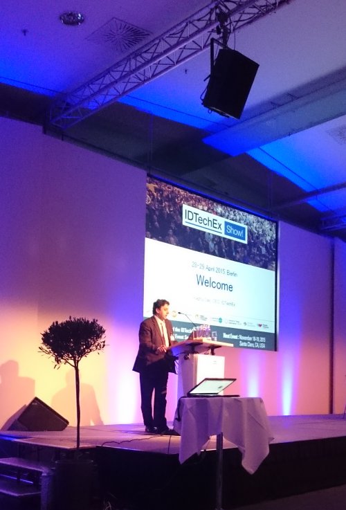
IDTechEx’s multi-track conference and exhibition explores the interconnected landscape of printed electronics, wearable technology, energy harvesting, the internet of things (IoT), graphene and 2D materials, 3D printing, and electric vehicles. Collaboration is key to succeeding in materials translation, and for me this was one of the big messages of the 2015 show, which brings together formulation specialists, systems developers, fabrication experts, measurement providers, and customer groups, all under the same roof for two days (or more if you sign-up to masterclasses).
Keynote welcome: Raghu Das, CEO of IDTechEx, briefs the audience on market projections for the printed electronics sector.
Dialogue between technology providers and end-users helps to resolve uncertainty in emerging fields such as printed and flexible electronics where – i) customers can be unsure about what’s possible and ii) suppliers need guidance on market requirements.
Bringing new technology to market
On day one, speakers from Qualcomm and Flextronics outlined how their firms bring new technology to the market. In Qualcomm’s case, its approach is built on four pillars – i) system R&D leadership, ii) design for manufacturability, iii) supply chain management and iv) customer support and engineering. It’s important not to overlook the final step. “The value proposition is only realized if you can propagate this to the customer,” Stein Lundby (R&D manager at Qualcomm) reiterated to audience.
Qualcomm, which Lundby describes as a ‘surface electronics’ company, is exploring opportunities for a hybrid product combining traditional crystalline based electronics with printed electronic components. Developed with Enfucell – a provider of printed power sources – the device features a 3-axis gyroscope and 3-axis accelerometer together with integrated battery and system electronics packaged in a band-aid style form factor. Users can stick the sensor on items such as golf clubs to determine how new products might improve their game, but this is just one possible scenario.
To navigate markets such as wearables, Flextronics – which focuses on production equipment and know-how – has opened design centres to help customers with product development and new use-cases such as electronic displays for athletic clothing. In his presentation, Keith Churches (head of innovation services at Flextronics) showed how the company brings new ideas to the market by configuring product-specific development networks that link the firm’s expertise with partners such as OEMs, universities and research institutes.
Nanomaterials Directa Plus – which was founded in 2005 and opened its graphene factory in 2014 – used the graphene and 2D materials conference track to talk through its collaboration with Vittoria Industries and highlight early market opportunities for graphene. Dubbed the wonder material, graphene – an ultra-thin layer of carbon – has been shown to have record-breaking electrical, thermal and mechanical properties, but breakthrough results in the lab don’t guarantee commercial success. “You have to be brave to be in the graphene market,” Giulio Cesareo (CEO of Directa Plus) commented.
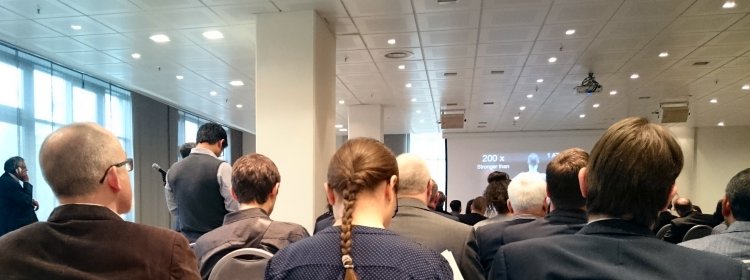
Full house: interest in graphene and related 2D materials remains strong.
Vittoria uses Directa Plus’ graphene nanoplatelets to formulate bicycle tyres and wheels with enhanced properties such as heat dissipation and lateral stiffness. There are 165 wheel makers in the world, Rudi Campagne (founder of Vittoria Industries) told the audience, and the use of nanomaterials such as graphene is an effective way for Vittoria to differentiate itself from the competition.
Early uses of graphene provide a platform for growth in other sectors by establishing a materials supply chain. Beyond tyres and wheels, Directa Plus is looking at opportunities for graphene in cleaning up contaminated soil and water. In his talk, Cesareo explained that linked graphene platelets have the potential to remove hydrocarbon pollution from lakes, according to test results. Literature from the firm claims that 1 gram of its Graphene Plus sorbent can adsorb up to 80-90 grams of oil – for more details, visit the GEnIuS project website, a programme co-founded by European Union within the Eco-Innovation initiative.
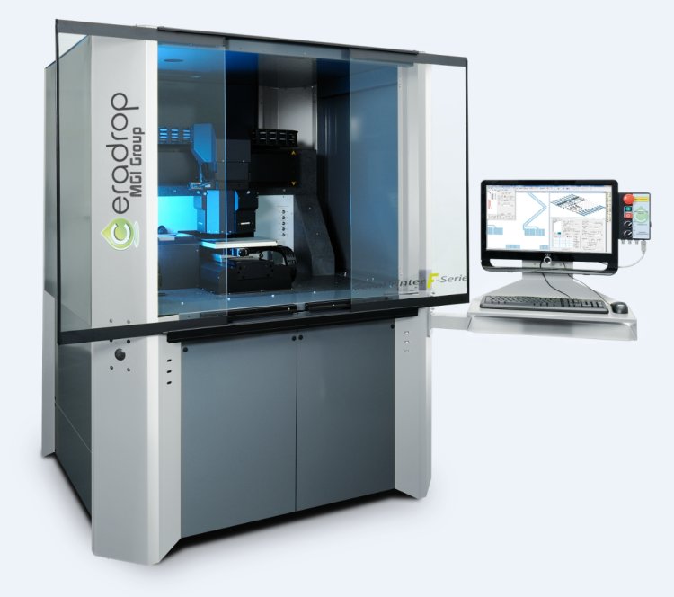
Exhibition: new products launched at the show included Ceradrop’s ‘F-Serie’ multi-material printer.
The discussion then moved on to opportunities for 2D materials in the electronics industry. If graphene does make an impact in this sector it is likely to be driven by novel applications, based on the views of the speakers in the opening session. “Graphene will not replace silicon in standard devices,” commented Guenther Ruhl (lead principal in new materials at Infineon Technologies) during his talk.
Touch screens are also looking unlikely as a big opportunity for graphene. “Graphene transparent conductive films are among the worst performers in a crowded market,” explained Khasha Ghaffarzadeh (head of consulting at IDTechEx). Like Ruhl, he feels that 2D materials could have more impact in new product categories. “The beauty of graphene is that there are many target industries and applications,” Ghaffarzadeh added.
OPV and R2R technology
Analyst events such as the IDTechEx show give attendees a view on tomorrow’s technology today. Two further highlights for me from the keynote presentations were Heliatek’s building integrated photovoltaics (BIPV) and Asahi Kasei’s e-beam fabricated seamless roller for printing transistors.
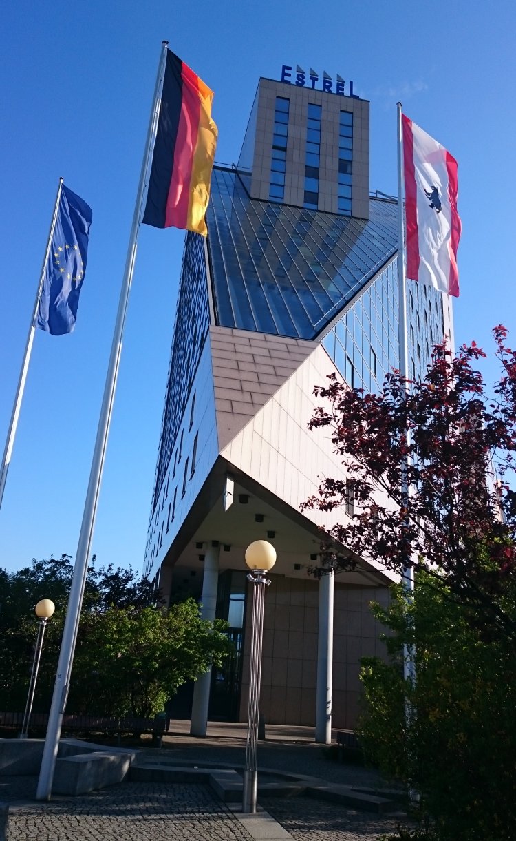
Show venue: Estrel, Berlin
In the afternoon on day one, Martin Pfeiffer (chief technology officer at Heliatek) outlined what he feels is a sweet spot for OPV – active facades. To compete with silicon, OPV has to bring something different, which it can when applications demand flexible and lightweight solutions. He added that the energy payback for an OPV cell can be as little as 3 months, as determined by the EU project dubbed X10D. Pfeiffer revealed that large-scale trials of the firm’s material were now underway in China and Germany on concrete (in Shanghai), PVC membrane (in Berlin) and glass (in Dresden) structures, with another pilot project due to start soon in Singapore on a glass and steel construction.
There were more glimpses of the future on day two when Masayuki Abe of Japanese giant Asahi Kasei – which operates in chemicals, electronics and healthcare sectors – presented his team’s work on seamless roller mold (SRM) technology for roll-to-roll (R2R) printing of sub-micron feature sizes. To make the mold, they rotated a super-smooth (2 nm roughness) roller under an e-beam writer. Moving the roller laterally (as well as rotating it) allows the team to create complex mold patterns. To test the process, Abe’s group used one of its roller molds to print a 200 ppi, 125 micron pitch TFT array. Abe was clearly proud of his team’s results and sees a bright future for the technique. “SRM will bring about the realization of high-resolution printing,” he told the audience.
Dates for your diary
The IDTechEx conference and exhibition takes place twice annually – once in Europe and once in the US (18-19 Nov 2015). The event returns to Berlin on the 27th and 28th of April 2016.
There’s plenty of talk about the hurdles that scientists have to overcome to commercialize their research, and while there’s nothing wrong in recognizing the scale of the challenge, it’s important to celebrate the success stories too. The Royal Society strikes a positive note in its recent video featuring Nanoco, Solexa and ARM, which offers advice on translating technology from the lab to the market.
Winning investment
The speakers are well placed to comment on the journey from discovery to devices, and each of them discusses different pieces of the puzzle, which includes raising money.
In the clip, Paul O’Brien, a professor at the University of Manchester and co-founder of Nanoco, emphasizes that the trickiest part to get funded is the step between invention and product development. To grab the attention of potential backers, it helps to think like one.
“The pull for the investor is the potential for a market,” O’Brien explains in the video. “So, if you can point towards a market like displays and say that [your product] could be in every house, in every country in the world, then they start to look interested.”
– You can find more videos from the Royal Society on its YouTube page
For additional case studies, check out the following articles from the journal Translational Materials Research –


