Lightning lab to offer full waveform testing by end 2014

Aerospace is a prime destination for materials that are both light and strong, but that’s only part of the story. Translating promising materials into production aircraft brings additional selection criteria into play such as the ability to survive lightning strikes. To find out more, TMR+ visited the Morgan-Botti Lightning Laboratory in Cardiff, Wales – one of the world’s leading facilities in this area.

Zap: high-speed video stills showing a composite panel under test. Credit: Morgan-Botti Lightning lab.

Zap: high-speed video stills showing a carbon composite panel under test. Credit: Morgan-Botti Lightning lab.

The primary focus of the £1.6 million centre, which was set up by Cardiff University in collaboration with AIRBUS Group Innovations, is on the electromechanical characterization of carbon composites, and its goal is to understand and develop safer and more lightning resilient materials.

Using banks of giant capacitors and resistor stacks, the custom-built lab can generate lightning strikes based on protocols such as the EUROCAE ED-84 Aircraft Lightning Environment and Related Test Waveform Standard.

Hot spots
Directing the centre’s activities is Manu Haddad from Cardiff University. In the tour, he explained that the tips of the aircraft such as the wings or nose tend to be targets for the initial strike, but because the plane is in motion the main fuselage will also likely come into contact with the discharge and needs to be protected too.

Samples from Morgan-Botti lightning lab

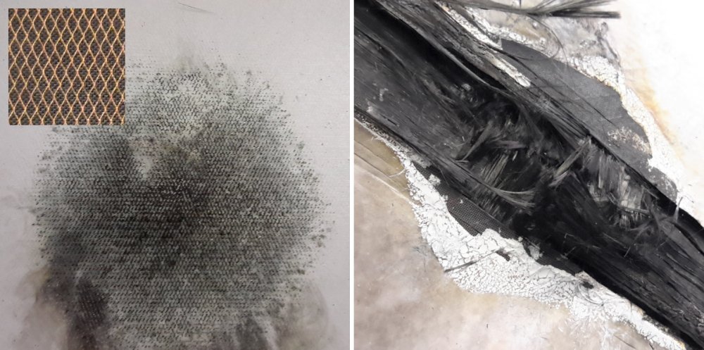
Test results: carbon composite samples with and without copper mesh (inset).

Today, aircraft makers such as Airbus and Boeing use a copper mesh bonded to the skin of the carbon composite material to disperse the energy from the lightning strike, but this adds weight – typically an extra 3% – and so developers are motivated to optimize their designs and find lighter-weight alternatives.

The lab’s measurement chamber is kitted out with thermal and high-speed cameras to evaluate the dynamic performance of test pieces, and the facility has access to a range of other characterization equipment including scanning electron microscopes.

Electromagnetic issues
Without protection, the top layers of the composite are ripped from the surface as the local area jumps in temperature, which risks overall mechanical failure. Also, designers need to consider the damage caused by electromagnetic radiation penetrating the material, where it could disrupt sensitive equipment below such as wiring loops or sensors.

Resistor stack and capacitor bank for generating lightning waveforms.

Resistor stack and capacitor bank for generating lightning waveforms.

Haddad illustrated how aircraft parts can be modified by showing a composite nose cone fitted with aluminium strips on either side to draw lighting strikes away from the radar equipment often housed in this portion of the plane.

Airbus is a major research partner and played a key role in the lab’s founding back in 2007 together with support from the Welsh government, but today the facility is supporting more than just the aerospace industry. “Wind turbines also need to be protected and we’re working closely with the energy sector on this,” commented Haddad.

Networking opportunities
To encourage collaborative research on the direct effects of lightning on emerging materials, Cardiff University is co-ordinating an international network of academic and industry partners dubbed EMC3 (Electro-mechanical characterization of carbon composites).

For more details on the lab and on becoming a member of the EMC3 network, contact Haddad and his team – lightning.engineering.cf.ac.uk/contact-us.html

Related reading

Lightning Hazards to Aircraft and Launchers (Aerospace Lab – Issue 5)

Lightning strike protection strategies for composite aircraft (Composites World)

AGU Fall Meeting 2014: Lightning never strikes twice? (blog.environmentalresearchweb.org)

Related links

Advanced High Voltage Engineering Research Centre (Cardiff University)

Video archive – lightning tests (Morgan-Botti Lightning Laboratory)

Registration opens for Young Technology Award bootcamp at COMS 2014, Utah

MANCEF’s commercialization of micro, nano, and emerging technologies conference (COMS) gives early-stage companies in these fields the opportunity for expert feedback through its Young Technology Award.

In 2014, the event takes place in Salt Lake City, Utah, and is hosted by the Center for Engineering Innovation.

Young Technology Award timetable

  • Sunday 12 October 2014, noon to 7 pm – expert bootcamp and pitch training
  • Tuesday 14 October 2014, from 6:30 pm – top six entrants go through to the Young Technology Award final held at the Natural history museum of Utah.

Focus on materials translation
Other highlights in the COMS 2014 program include a session chaired by the journal Translational Materials Research (Track C4 – Tuesday 14 October, 2 pm) looking at progress in the commercialization of devices based on graphene, and exploring the acceleration of materials translation through innovation ecosystems.

Related stories
Gearing up for the commercialization of micro- and nanotechnologies (TMR+)
Show report: COMS 2013 (nanotechweb.org)

NSF expands I-Corps innovation network for translating academic research into the market

The National Science Foundation (NSF) is further extending its popular I-Corps innovation network with nodes in Texas and Southern California.

Now in its 4th year, the I-Corps program brings together academic researchers, student entrepreneurs and business mentors to focus on the transition of technology from the lab to the market. The scheme features a mandatory I-Corps curriculum that examines the transfer of knowledge into products and processes that benefit society, and introduces the concept of a Lean LaunchPad.

To fulfil the latest expansion, the NSF has awarded two grants of $3.75 million, each over three years, to consortia based in the two regions. The Southern California node will be based at the University of Southern California (USC) and includes the University of California Los Angeles and the California Institute of Technology (Caltech). The Texas hub, known as the Southwest Alliance for Entrepreneurial Innovation Node, will be based at the University of Texas at Austin and includes Rice University and Texas A&M University.

Existing I-Corps regional nodes –

  • Washington, D.C.
  • New York City,
  • Michigan,
  • Northern California
  • Atlanta

New additions to the network –

  • Southern California
  • Texas

Accelerating biomedical innovations
Earlier this year the NSF joined forces with the National Institutes of Health (NIH) to deliver a program aimed at accelerating the translation of biomedical innovations into applied health technologies, which goes under the name of The I-Corps at NIH.

Related links

Video: team members describe the I-Corps experience (NSF)

UT, A&M, Rice Form NSF hub to move ideas to marketplace (University of Texas at Austin)

USC teams with UCLA and Caltech on federally funded innovation hub (University of Southern California)

Video highlights from Graphene Week 2014 (Gothenburg, Sweden)

Graphene Week is now the annual showcase event for Europe’s Graphene Flagship programme – a 10 year, Euro 1 billion initiative that hopes to accelerate the translation of the so-called wonder material from lab to market. For attendees, the five-day conference is a chance to find out what big names in the field such as Nobel-prize-winner Andre Geim think about graphene’s prospects.

As Geim observes in the clip, currently applications are focused on using graphene as a substitute to other materials. But what he’s really looking forward to are applications unique to graphene – uses where the 2D allotrope of carbon performs a function that no other material can achieve.

Other experts at the event included leaders of the Flagship’s 16 work packages (WPs). Andrea Ferrari (WP 5 – Optoelectronics), who’s based at the Cambridge Graphene Center, sees graphene’s optical properties as beneficial for shaping laser pulses and creating photodetectors that operate in the infrared.

Joining Ferrari on WP 5 is Frank Koppens – group leader at ICFO in Barcelona. Koppens is already talking about building prototypes and taking devices out of the lab to demonstrate the industrial relevance of graphene in areas such as automotive night vision.

Continue reading

Show report: Graphene supply, application and commercialization 2014 (Manchester, UK)

It’s been 10 years since graphene was isolated by Geim and Novoselov at Manchester University in the UK. Today, graphene is available to purchase from a range of suppliers, you can buy equipment for growing it on wafers and foils and you can find graphene in products on the market, but the so-called “wonder material” is still in the early stages of its commercial journey.

Taking shape: the National Graphene Institute at Manchester, UK. The state-of-the-art facility is due to open in March 2015, but staff will start moving in from October this year to begin proving out the building services.

Taking shape: the National Graphene Institute at Manchester, UK. The state-of-the-art facility is due to open in March 2015, but staff will start moving in from October this year to begin proving out the building services.

“Short term applications will pave the way towards the principal uses of graphene,” Jani Kivioja, head of nanomaterials at Nokia, told attendees at LBC’s popular graphene conference series – now in its second year – which examines prospects for the 2D allotrope of carbon from an industrial perspective.

Early wins
TMR+ has reported graphene’s use as an additive to prevent drilling fluid degradation at high-temperature (see – Agensi Inovasi Malaysia and Graphene Nanochem team up to develop innovation hub), and there were other early wins presented at the event. Ready-for-market examples included a transparent conductive coating from TBA, which provides electrostatic discharge (ESD) protection to industrial lighting in explosive environments such as oil refineries or mining works (see TBA case study – PDF).

Graphene coatings are also of interest to Tata Steel, another attendee at the meeting. The firm sees the material’s barrier properties as an option for delivering anti-corrosion performance and extending the lifetime of its major products.

Plastic fantastic
Other areas with market potential include composite materials, where graphene’s high strength makes it an attractive additive. Its sheet-like form is beneficial during processing as graphene platelets flow easily over each other unlike carbon nanotubes, which can knot together and make composite mixtures much more viscous and harder to manage.

Karl Coleman, a professor at Durham University and one of the founders of Applied Graphene Materials, added that graphene is very good at reducing nitrogen permeation in thermoplastics, which is of interest in the packaging sector. Also, the low loading levels required preserve colour and transparency in the host material, which can be significant. Coleman is involved in Grapol, a four year project sponsored by EPSRC and partnered by Proctor and Gamble, and Dyson – two big consumers of thermoplastics.

As Coleman and others highlighted the effective integration of graphene into host materials is strongly dependent on surface functionalization, which is an area that suppliers such as Haydale are targeting with their plasma-treated graphene nanoplatelets. Surface functionalization also opens the door to the use of graphene in sensing applications, a sector that Nokia was upbeat about.

But will this be the killer application? For graphene to really take off there is a sense that it has to offer something different, something that no existing material on the market can do.

“Where I believe graphene can make a difference and be potentially disruptive is through its multifunctionality,” commented James Baker, who has moved from BAE Systems to become business director at the UK’s National Graphene Institute (NGI) – a £61 million facility under construction at Manchester University.

Graphene is unique in possessing so many record-breaking properties, but as we’ve mentioned previously on TMR+, designing multifunctional components to capitalize on this requires significant developer resources (see – Trajectories in translation: parallels between old and new materials) and pushes out the timeline for translating breakthroughs into the marketplace.

Facilities such as the NGI intend to bring academia and industry together under one roof to accelerate the commercialization of graphene from technology readiness levels 3-5 into early process validation. In September 2013, graphene CVD expert Bluestone signed up as the NGI’s first strategic partner and the building is on track to open in Q1 2015.

Reality check
Achim Hoffmann of IP group, a UK-based team of investors bridging the chasm between science and the city (financial district), reminded attendees that graphene is “technology before application”, which adds to the challenge. “We invest in businesses and value propositions – not materials,” emphasised Hoffmann. “Start-ups need to focus on who their customer is and how they address the market.”

Dispite the difficulties, a commercial landscape for graphene is emerging. Mark Rahn of MTI Ventures, who also spoke at the event, estimates that there are 23 countries (at least) with graphene companies. Europe hopes to be a major player through its Graphene Flagship, and across Asia there’s a wave of companies now making graphene in some shape or form – a point made by Kitty Cha of BASF and echoed by my colleagues at IOP China.

Device development
Seungmin Cho was representing Samsung Techwin at the workshop and talked about his team’s work on transparent electrodes. Using a graphene/PET film created by roll-to-roll processing, the group has demonstrated the manufacture of fully functional 4” touch screens – see ACS Nano 8 (2014) – but whether these devices make it into full production remains to be seen. “We need to find something that ITO cannot do,” Cho told the audience.

I got the impression from Shu-Jen Han’s presentation that graphene could be a hard sell in digital logic chips too. Han is a master inventor at IBM’s Yorktown Heights site in the US. The lack of a band gap in graphene means that devices are hard to turn off (in other words, you can write 1’s, but it’s tricky writing 0’s). There are ways of modifying the material to get around this, but from a commercial perspective the additional steps required are unattractive.

RF electronics on the other hand could be a much better match for the material. “For analogue devices you don’t have to turn the transistor fully on or fully off,” he explained. The IBM team has built a test circuit that can demodulate a digital signal carried over RF – see Nature Comm. 5, 3086 (2014). What’s more, the graphene chip was stable across a wide temperature range and up to high temperatures, which differentiates the device from versions made using traditional semiconductors.

Large organizations taking an interest in graphene include Lockheed Martin, which sees water security as a key part of its future business and believes that the 2D material could play an important role. To explain, Steve Sinton – principal chemist and Lockheed Martin fellow – introduced his team’s work on a perforated graphene membrane dubbed “Perforene”, which is seen as a promising platform for water purification (see datasheet – PDF). The work is early stage, but already the group has demonstrated that “Perforene” can reject salt ions from a test solution and copper from industrial wastewater, which has potential benefits in areas such as the electronics industry.

These are just a few highlights from what I found to be an insightful two days of talks and discussion. For further details on the event visit – www.graphene-applications-2014.com – and for more on graphene, check out the links below.

Related content on the web –

RESOURCES

Graphene: fabrication methods and thermophysical properties (Physics-Uspekhi)

Graphene: Applications and future uses (IOP)

Graphene coverage on nanotechweb.org

Graphene circuit ready for wireless (IBM Research blog)

COMPANIES

Aixtron # Applied Graphene Materials # Bluestone # Cientifica # Graphoid # Haydale # Ocsial # Perpetuus # Planartech #

MC10 declares that the future of electronics is flexible

In my view, the concept of stretchable electronics that can be integrated with clothing and the human body could bring revolutionary technologies and spawn new industries. I’m a journalist working for Physics World magazine and I’ve recently produced a short film on this topic, which I’m delighted to share with TMR+. The video report takes you inside the headquarters of one of the most exciting companies in this burgeoning technology area — a start-up called MC10 based in Cambridge, Massachusetts.

One of the company co-founders is John Rogers of the University of Illinois at Urbana-Champaign, a pioneer in the field of flexible electronics. In the film Rogers talks about how his interest in the research emerged from the observation that all known forms of biology are soft, elastic and curvilinear, whereas existing forms of electronics are rigid planar and brittle. “As a result, if you want to integrate electronics with biology – with human skin or tissue – you have severe challenges in a mechanics mismatch and a geometrical form mismatch,” he says.

Translation tool
Rogers talks about how MC10 has overcome these mismatches by developing a printing process that allows devices to be built on rigid wafers before being lifted off in thin formats and then printed onto rubber substrates. This innovation is enabling the company to develop professional and consumer products based on integrated electronics that can flex and reshape in a range of different environments.

The film profiles one of the company’s products called the Reebok CHECKLIGHT, developed by MC10 in partnership with the sports equipment giant whose global headquarters is also in Massachusetts. It’s a type of skullcap that can be worn by athletes and provides an indication of the danger of head impacts, through the combination of an accelerometer and a gyroscope integrated into flexible materials. The product has an interesting backstory about the concerns among youth athletes and trainers about the risk of serious injuries. For example, in sports such as American football, there tends to be something of a hero culture whereby players will respond to head collisions by saying “I’m fine coach”, even if they’re really not. The Reebok CHECKLIGHT is designed to provide an objective assessment of head impact in that scenario.

Creative environment
We recorded the film over a couple of days at the end of last year, when I visited the MC10 headquarters with a small film crew. The experience certainly lived up to my expectations of what a dynamic start-up in this part of the world would be like. Alongside the labs and the business spaces, the office also had many classic start-up accessories such as running machines and a range of gourmet coffee on tap. Perhaps these mod cons go some way to explaining the friendly and co-operative nature of the MC10 people we interviewed. For example, one of the co-founders Roozbeh Ghaffari was more than happy to model the Reebok CHECKLIGHT for us by popping it onto his own head without a moment’s hesitation. From my experience – particularly with British academics – this type of thing normally takes a bit of persuasion!

Equally amenable was Benjamin Schlatka, the VP of Business Development who appears in the film talking about his personal interest in the products of MC10. As a parent of three children his interest was piqued by the idea of a wearable sensor that could measure the temperature and respiration of a child while it sleeps. Schlatka goes on to talk about the key business developments in the history of MC10, which was established in 2008 after John Rogers established a connection with an entrepreneur in the Boston area.

Rather than me spoiling the film anymore, I recommend you give it a watch!

Note – John Rogers is a founding board member of the journal Translational Materials Research (TMR).

Related reading on the web –

Nanoarray patch takes your temperature to millikelvin precision (nanotechweb.org)
Silk helps make bio-integrated electronics (nanotechweb.org)

Interview with George Grüner, Editor-in-Chief of Translational Materials Research

George Grüner Distinguished Professor of Physics, University of California, Los Angeles

George Grüner Distinguished Professor of Physics,
University of California, Los Angeles

How do you define translational research?
Translation is the series of innovations that are needed to advance fundamental discoveries or inventions into useful products. This raises a number of issues that are not usually discussed in the invention or discovery phase: scalability of fabrication, reproducibility, lifetime, packaging, and yes, the price.

Why the focus on translation?
Within the academic community the nature of research is rapidly changing. More and more the expectation is that scientific endeavours will lead to practical applications, with funding often directed towards a specific goal with a clear value proposition. As a result, universities have become more focused on innovation, and are now developing intellectual property that can be marketed to the enterprise sector.

What is meant by the “valley of death”?
One meaning is simple: death occurs when a company developing a product runs out of money. But there is another definition: the valley of roadblocks that an invention must be pushed through until a viable product emerges. There are many roadblocks, many potential setbacks, many ways a technology can fail, thus the name the valley of death.

How will the journal Translational Materials Research (TMR) connect the different stakeholders in the innovation chain?
Our aim is to discuss issues that are relevant to all stakeholders involved in translation. Articles cover not only advances in technology, but also the steps needed to develop a marketable product. Our Editorial Board also represents the broader community, with company CTOs and venture capitalists sitting alongside leading scientists from academia and industry.

What would you say to authors who are considering publishing their work in TMR?
My hope is that TMR becomes a vital source of information for all those scientists who dream of launching a company and changing the world. Publishing your work with TMR will help all those people to achieve their dream.

Materials translation wins Euro 1 million prize

Stuart Parkin has been named winner of the 2014 Millennium Technology prize – a € 1 million award highlighting innovations that have made a positive impact on society and are stimulating further cutting edge research and development. The prize recognizes Parkin’s contribution to the translation of the giant magnetoresistance effect from the discovery that won Albert Fert and Peter Grünberg the Nobel prize for Physics (in 2007) into a technology platform for high-capacity magnetic disk drives.

Atomically engineered materials
Parkin’s work on thin magnetic films has enabled disk-drive makers to configure read-heads that can detect much smaller regions of digital information, and has allowed developers to increase storage capacity as a result.

His win has been celebrated across the web. Coverage includes stories on the BBC and Wired, but fans of materials translation will probably enjoy Parkin’s interview with The Guardian most of all –

“I showed that you didn’t need these very exotic techniques but one could actually [use] a much simpler technique which was compatible with mass manufacturing,” he told the news organization.

Speaking via a video link on the day of the announcement, Parkin said that future plans for his research team include developing computing architectures that would allow much more energy-efficient processing of information.

Stuart Parkin is a fellow of The Institute of Physics and a founding editorial board member of TMR+’s sister journal Translational Materials Research.

Useful links –
The spin on electronics (online lecture given by Stuart Parkin, Nov 2013)

Show report: Metal additive manufacturing 2014 (Sheffield, UK)

As promised in the flyer, the Association of Laser Users (AILU) event brought together a mix of additive manufacturing (AM) experts from industry and academia to discuss the tough topics that are all too often ignored in the media hype surrounding 3D printing. Split into four sessions, the meeting was chaired by Robert Scudamore from manufacturing and fabrication consultants TWI.

Setting the scene
The aerospace sector is a prime candidate for lightweight, lattice structures that are easy to build using AM tools. Also, 3D printers enable a high-level of part customization, which benefits medical implants and patient-specific surgical tools. But both aerospace and medical sectors require significant materials and process qualification.

Also, there are setup costs to factor in. Additive techniques such as 3D printing use much less material than subtractive processes such as milling, but the initial materials outlay can still be high. For example, filling an industrial laser sintering machine with virgin titanium powder can cost thousands of pounds.

Speed of production is another issue, with some parts taking hundreds of hours to build.

Reality check
One of the first speakers to start busting the myths was Robin Wilson from the UK’s Technology Strategy Board (TSB). “Additive manufacturing is not just printing from CAD,” he told delegates. Potential users need to consider the whole process, which as Wilson points out involves a significant “digital data supply chain” and physical “post-processing” of the finished component.

Stéphane Abed of Poly-Shape, who also spoke at the meeting, manufactures parts using a tool path that co-ordinates four beams. These multiple lasers can build several smaller components at once or construct different sections of a single work-piece simultaneously, to improve production rates. But having multiple optical-trains also ramps up the number of variables in the process.

Listening to the presentations, it’s clear that AM has no shortage of parameters that influence the quality of the manufactured part – laser power, writing speed, powder flow rate (for nozzle-blown setups), particle size distribution and recycle rate, are just a few.

It can be done
Throughout the day, process control remained a key talking point. Trevor Illston of Materials Solutions, who led the final session of talks, is optimistic that AM can be controlled to a “production standard” by inspecting workpieces at multiple points in the AM process.

Giving the audience food for thought, Illston added that there can be a downside to the design freedom that 3D printing brings to the table, as it’s possible to create parts that are incredibly difficult to examine!

In general though, unlocking traditional design constraints is a big win for AM – and despite the production challenges, all of the speakers recognized that major opportunities are up for grabs.

The medical sector is a growth area for AM, not just for implants, but also for custom tools such as cutting blocks to guide surgery. Medical centres are looking at options for manufacturing parts in hospital to speed up delivery to the patient. Ideas here include flat-packed production tools that can be sterilized and then assembled in theatre.

“AM often solves one problem beautifully, but it can create other issues,” said Edward Draper of JRI Orthopaedics, who spoke in the opening session. Draper picked up on Wilson’s earlier remark about post-build processing, and emphasised the requirement for cleaning and polishing.

Something new
Images of medical devices, helicopter components and fixtures for satellites are becoming a familiar sight at AM conferences and events, but Neil Burns of Croft Engineering had something new for the audience – filtration parts. Traditionally, Croft Engineering has made filtration supports by shaping wire mesh, but the bending process leads to apertures that are non-uniform. To get around this, Burns showed how his company uses AM (inspired by a trip to Fab Lab in Manchester, UK) to build filtration supports with holes that are aligned to the direction of fluid flow – a design feature that saves customers money by reducing the amount of energy that’s required to pump liquid through the component. Despite the benefits, Burns revealed that clients can be cautious about using AM parts. They fear downtime caused by mechanical failure.

But what is the effect of AM on materials performance? How do AM samples behave under load compared with material that has been cast or milled? AM components might look fine on the outside, but what’s happening to the internal structure of the material? Also, how does the strength of parts made using different machines compare, or parts that are built on the same machine, but formed using a different tool path, or using powders with a different particle size distribution or storage history?

Team effort
To tackle this, AM needs its own materials database and standards – a point made by many attendees, including Neil Mantle of Rolls-Royce. What’s more, the task requires a collaborative effort. Contributions so far include EU initiatives such as SASAM (Support Action for Standardisation in Additive Manufacturing) and the UK’s ANVIL project to establish benchmarks and design guides for AM.

A continuing development is the use of technology hubs to support AM projects at technology readiness levels (TRL) 4-6, or in other words to translate projects from proof-of-concept to pilot-scale operation.

David Wimpenny from the UK’s Manufacturing Technology Centre (MTC), which was established in 2010 to bridge the gap between academia and industry, was at the event. “Our role is to make parts that industry can relate to in terms of size and quality,” he explained.

Today, the MTC is part of the UK’s high value manufacturing (HVM) catapult – a network of seven technology centres with a shared goal of accelerating process innovation.

Related links –

Metal Additive Manufacturing: opportunities in applications and improvements in process technology (full programme)

Supply chain knowledge: formulating and applying new materials

Carbodeon is a supplier of carbon-based additives including detonation produced nanodiamonds (4-6 nm) that offer major upgrades in materials performance, but success in this sector isn’t as straightforward as simply demonstrating record-breaking properties.

“You have to create a situation where delivery is beneficial for everyone in the supply chain otherwise the material won’t make it to the end user,” Gavin Farmer, business development manager at Carbodeon, told TMR+.

Considerations include materials cost, availability and impact on manufacturing.

Nanodiamond is available in dispersions, suspensions and powdered forms (credit: Carbodeon)

Nanodiamond is available in dispersions, suspensions and powdered forms (credit: Carbodeon)


The firm offers chemically-treated nanodiamonds as suspensions (of small agglomerates) and dispersions (of individual particles) that can often be mixed directly with raw materials, and reduce the amount of specialized knowledge required by the customer. Powdered forms are also available, but typically the integration step takes longer to optimize.

For Carbodeon, the split between nanomaterials development and applications-related research is roughly 70/30.

Adoption by industry
The company provides samples of material to clients for assessment, but for this approach to succeed the customer must be willing to enter into a series of experiments and have the tools to validate the results. Also, clients may lack the deep scientific knowledge that could be required to absorb the technology, and require further support.

Where a strong market opportunity exists, Carbodeon will push further into the application area and pursue patent opportunities. This opens the door to licensing revenue and gives added value to the customer through exclusive use rights.

“Whenever you invest in applications-related research, you need to make sure that you can monetize the work,” adds Farmer.

Product development
Success stories for Carbodeon so far include electroplating, where nanodiamonds have been shown to nucleate grains of the coating material, which reduces cracking and ramps up the corrosion protection offered by the electroplated layer. The embedded particles also improve wear and reduce friction thanks to their materials properties.

A notable characteristic of diamond is its very high thermal conductivity, which is rare for materials that are electrically insulating. Carbodeon is working with developers to formulate superior thermal interface material (TIM) and easy-to-process heat sinks for managing cooling in electronics.

“We’ve taken polymers that contain thermal fillers, typically micron-sized boron nitride or alumina particles and milled them with nanodiamond (0.1% by weight),” said Farmer. “The much smaller diamond particles bridge gaps in the filler network to boost thermal conductivity by 25%.”

Driving down emissions
The firm’s latest product is dubbed uDiamond Vox D – a formulation that Carbodeon claims can double surface durability and reduce friction by up to 66 percent.

Pre-functionalized with a surface chemistry tailored to suit PTFE, the liquid dispersion of nanodiamonds can be mixed directly with industrial fluoropolymer coatings ready for application by spray or screen printing with little or no change to the process parameters.

“In automotive powertrains alone, the fuel and CO2 savings through friction reduction will make a real difference,” commented Farmer.

Further reading on the web –

Carbodeon Oy: Better heat conductivity extends equipment lifespan (Tekes)