Argonne launches Nano Design Works to support materials commercialization and accelerate the translation of research into products

Argonne National Laboratory has launched Nano Design Works to amplify the impact of its expertise in nanotechnology. Last year, Argonne interacted with more than 600 companies, and hubs such as the Center for Nanoscale Materials offer developers a wealth of scientific knowledge and instrumentation.

Open for business
Dubbed a ‘concierge’ service, Nano Design Works caters for businesses of all sizes to match-make clients with Argonne expertise. “We work with industry partners to solve their enduring R&D challenges, identify commercialization opportunities, license new technologies, and introduce transformational discoveries to the marketplace,” Andreas Roelofs, director of Nano Design Works, told TMR+. “Project scale and duration is flexible, ranging from single-day solutions to multi-year investigations.”

Financing
A variety of funding mechanisms are available for companies to work with Argonne, including securing investment from government agencies and venture capital firms through collaborative proposals. “We think that bringing together the world-class resources of Argonne with the ability of companies to commercialize breakthrough science will be appealing to potential funders,” said Roelofs.

Drugs that use nanotechnology to target only cancerous cells while leaving healthy cells untouched; magnetic nanofibers that could create new, more powerful antennas or be used for novel sensors and dectectors; and nanodiamonds that combine with graphene to create nearly frictionless surfaces, are just a few examples of projects that Nano Design Works is currently engaged in.

Related links

Call for papers: Focus on 2D materials beyond graphene
Which applications are likely to benefit the most from emerging 2D materials and what distinguishing properties are required to enable novel functionalities or novel devices and products?

An interview with board member Peter Littlewood
National labs are well placed to work the middle ground between academia and industry to find solutions to big problems. Peter Littlewood, director of Argonne National Laboratory, talks about his approach to tackling major issues such as energy storage and sustainability.

Infographic: smart materials classified by application and development stage

Lux Research has tracked the translation of smart materials from the lab to the market in its latest report – ‘Get Smart: smart materials as a design paradigm’ – examining advances in the development of smart materials and their adoption by industry.

Smart materials from lab to market: classes, applications and development stages [image credit: Lux Research]

Smart materials from lab to market: classes, applications and development stages – for a larger version of the infographic, click on the image [image credit: Lux Research]

Long incubation times, but rapid commercialization when conditions are right
As you’ll discover by reading TMR+ (most recently in this month’s story on OLEDs) – translating promising results into a robust products can take decades and smart materials are no exception, according to the Lux analysis.

What’s also interesting to note is the rapid pace of commercialization once market conditions are right – pieozelectric materials are a great example. This class of materials was long relegated to niche applications before booming due to adoption in mainstream products such as inkjet printers, digital cameras and smartphones, as Anthony Vicari – lead author of the report – points out.

Related reading on TMR+
Partnerships and revenue models unlock opportunities for smart coatings
Trajectories in translation: parallels between old and new materials

DuPont gearing up for OLED to become display standard

DuPont is scaling up its formulations capability in the area of OLED materials. Recently, the chemicals giant has opened a facility to serve the commercialization of next-generation TVs and other large-format displays. The firm has invested more than $20 million in the plant, which is based at DuPont’s Stine-Haskell Research Center in Delaware, US.

Technology package
Back in June, DuPont announced that it was teaming up with Kateeva, a manufacturer of industrial ink-jet printing equipment, to optimize materials and processes to advance the fabrication of Organic Light Emitting Diode (OLED) displays.

Printed displays give developers the opportunity to reduce material waste compared with evaporative techniques and target more competitive price-points for their products.

Applications for OLED materials also include lighting, and DuPont is working with the Holst Centre on this topic as part of an extended collaboration reported in 2014.

Timeline
DuPont has been building its portfolio of OLED materials for 15 years. In 2000, the firm acquired UNIAX – a pioneering display company founded by Alan Heeger, which was spun out of the University of California, Santa Barbara (UCSB) in 1990. Heeger is a winner of the 2000 Nobel Prize in chemistry (together with Alan G. MacDiarmid and Hideki Shirakawa) for the discovery and development of electrically conducting polymers.

Related stories on TMR+
How can you reduce the cost of flexible electronics?

Related articles from the journal Translational Materials Research (TMR)
Organic electronics: Europe builds TOLAE portfolio to address markets (Transl. Mater. Res. 2 030302)
An interview with board member Serdar Sariciftci (Transl. Mater. Res. 2 010202)
Singlet harvesting copper-based emitters: a modular approach towards next-generation OLED technology (Transl. Mater. Res. 1 015003)

Arkema emphasises 3D printing in its materials research agenda

Layer-by-layer fabrication has long been used for industrial prototyping, but a boom in lower-cost, desktop 3D printers is broadening its appeal and materials suppliers are responding as markets for these versatile tools expand.

Polymer pellets. Image credit: Arkema.

Polymer pellets. Image credit: Arkema.

This week, Arkema – whose company history goes back to a reorganization of Total’s intermediate chemicals group in 2004 – announced that it is adding 3D printing as a 6th ‘innovation driver’ for its international research and development (R&D) operation. ‘Materials for 3D printing’ joins existing R&D programmes in ‘lighter materials’, ‘renewable raw materials’, ‘materials for energy’, ‘water treatment solutions’ and ‘materials for electronics’.

Arkema offers polymers for laser sintering as well as UV-curable resins, and is developing formulations that can be used to make extremely tough 3D-printed products. But it’s not just the big firms that are busy innovating and ramping up the range of materials available to the growing 3D printing community. Materials start-ups and university labs are also participating in the translation of novel feedstock.

In fact, a web-search reveals a curious array of 3D printable materials, which includes coffee (3Dom USA), coconut (Formfutura), seaweed (University of Wollongong) and graphene (Black Magic 3D).

Related stories on TMR+
Materials and equipment upgrades add to 3D printing’s appeal

Related articles in the journal Translational Materials Research (TMR)
What can 2D materials learn from 3D printing? (Andrew Haughian 2015 Transl. Mater. Res. 2 020201)

Related stories on the web
A*STAR’s IMRE invents highly conducive material for 3D-printing of circuits
Oxford Performance Materials launches 3D printing technology for aerospace and industrial applications

US funding round up: multi-million dollar awards for flexible hybrid electronics, nanotechnology and advanced materials translation

It’s been a big couple of months for materials science funding in the United States. TMR+ rounds up the key announcements.

Flexible hybrid electronics
AUG 2015 – the US Department of Defense (US DOD) has awarded $75 million to the Flextech Alliance to establish and manage a Flexible Hybrid Electronics Manufacturing Innovation Institute (FHEMII).

The Flextech Alliance has created a map (JPEG format) of its 150+ partner network, which clusters around nano-bio; flex substrates; design, modelling and testing; equipment and materials; deposition and printing; CMOS thinning; packaging; and standards.

According to the announcement, the funding, which runs for five years, will be matched by more than $96 million in cost sharing from non-federal sources, including the City of San Jose, private companies, universities, several U.S. states, and not-for-profit organizations.

Beyond defence applications, other markets for flexible hybrid electronics include automotive, communications, consumer electronics, medical devices, health care, transportation and logistics, and agriculture.

Nanotechnology
SEP 2015 – the US National Science Foundation (NSF) is providing $81 million over five years to support 16 sites and a coordinating office as part of a new National Nanotechnology Coordinated Infrastructure (NNCI).

The NNCI framework is the successor to the National Nanotechnology Infrastructure Network (NNIN), which – as the program synopsis outlines – provided researchers from academia, small and large companies, and government with open access to university user facilities with leading-edge fabrication and characterization tools, instrumentation, and expertise within all disciplines of nanoscale science, engineering, and technology.

Advanced materials translation
SEP 2015 – Designing Materials to Revolutionize and Engineer our Future (DMREF) is the NSF’s ‘primary program’ for participating in the Materials Genome Initiative – a multi-agency initiative to accelerate advanced materials discovery and deployment by exploiting advances in computational techniques, and making more effective use of standards, and enhanced data management.

Recognizing the multi-disciplinary nature of the task, DMREF reaches across various NSF directorates including Mathematical and Physical Sciences; Engineering; and Computer and Information Science and Engineering.

DMREF funding consists of 20 – 25 grants of between $750,000 and $1,600,000 to develop, for example, new data analytic tools and statistical algorithms; advanced simulations of material properties in conjunction with new device functionality; advances in predictive modeling that leverage machine learning and data mining; and new collaborative capabilities for managing large, complex, heterogeneous and distributed data.

Related stories on TMR+
Materials by design: NIST announces consortium to speed up time from discovery to first commercial use
Show report: IDTechEx Printed Electronics Europe 2015 (Berlin)

MESA+ advanced materials spin-off receives EURO 1 million from Cottonwood Technology Fund to scale up ‘flexiramics’

Eurekite, an advanced materials spin-off from the University of Twente in the Netherlands that refers to its non-brittle, nanofibre-based products as ‘flexiramics’, has attracted a EURO 1 million investment from Cottonwood – a US venture capital (VC) firm with a European hub in Twente’s largest city, Enschede. The university start-up plans to use the VC funding to deliver prototypes based on its 100% ceramic materials, which were first developed at the MESA+ Institute of Nanotechnology, and to scale-up its operation.

Designer material: flexible 100% ceramic developed at MESA+ and available via Eurekite – a spin-off from the University of Twente. Image credit: Eurekite

Designer material: flexible 100% ceramic developed at MESA+ and available via Eurekite – a spin-off from the University of Twente. Image credit: Eurekite


“We have created a material that merges the properties of paper and ceramics,” says Eurekite co-founder Bahruz Mammadov (COO/CFO) who formed the company less than a year ago together with Gerard Cadafalch (CEO). Andre ten Elshof, a senior faculty member at MESA+, joins them as chief scientific officer. The team has strong connections to research programmes at the University of Twente investigating the properties of electrospun ceramic nanofibers. Based on promising results in the lab, the team decided to explore commercial opportunities for these tough and flexible nanomaterials.

Like conventional ceramics, Eurekite’s products don’t burn, but as the name suggests ‘flexiramics’ are much less fragile than traditional formulations and don’t shatter when dropped. The team hopes that this rugged combination of properties will inspire designers, and potential applications include high-temperature oil & gas sensors, flexible substrates for mobile phone antennas, lithium-ion battery energy performance upgrades, high-power electronics for electric vehicles and solar energy – to name just a few uses for ‘flexiramics’!

Ecosystem built for translation
As TMR+ witnessed on a tour of the region back in 2013, the University of Twente offers a healthy ecosystem for translating materials research from the laboratory through to the market. In addition to MESA+, local facilities include a prototyping environment (NanoLab) and the nearby High Tech Factory where early-stage companies can ramp-up to higher production volumes.

Related stories on TMR+
The dash for cash: a new funding landscape for high-tech start-ups
Gearing up for the commercialization of micro- and nanotechnologies

Related articles from the journal Translational Materials Research (TMR)
Sizing up your innovation ecosystem (Deborah Jackson 2014 Transl. Mater. Res. 1 020301)
Rethinking universities as innovation factories (Ralph M Ford et al 2014 Transl. Mater. Res. 1 016002)
A lab-to-market roadmap for early-stage entrepreneurship (Jesko von Windheim and Barry Myers 2014 Transl. Mater. Res. 1 016001)

Business school mines big data for clues on graphene commercialization

What can web scraping reveal about the commercialization of graphene? That’s the question Philip Shapira, Abdullah Gök and Fatemeh Salehi Yazdi have set out to answer using a mixture of computerized data mining and other analytical techniques.

The team, based at Manchester Business School, has chosen graphene as a ‘demonstrator’ to road-test its approach, which identifies patterns from publicly available information hosted on enterprise websites. The hope is that these methods can assist in providing ‘real-time intelligence’ to map the development of rapidly emerging materials and technologies.

In the pilot study, Shapira and his colleagues have focused on a set of 65 graphene-based small and medium-sized enterprises (SMEs) based in 16 different countries – 49.2% of the SMEs in the sample are located in North America, 15.4% in the UK, 18.5% in Western Europe and 16.9% in East Asia and emerging nations. The researchers acknowledge that they haven’t captured every graphene SME in every country, particularly in China, and note this under-representation should be kept in mind when comparing across the regions.

Presenting their findings in a Nesta working paper, the authors draw attention to the following –

  • Access to finance and the firms’ location are significant factors that are associated with graphene product introductions.
  • Patents and scientific publications are not statistically significant predictors of product development in their sample of graphene SMEs.
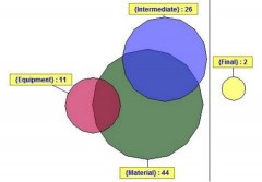
  • Graphene SMEs are focusing mainly on upstream and intermediate offerings in the value chain.
Relationship between different value chain positions of SMEs in the study. Credit: Nesta Working Paper 15/14

Relationship between different value chain positions – [equipment:11] [material:44] [intermediate:26] [final:2] – of SMEs in the study. Credit: Nesta Working Paper 15/14

Graphene advantage?
According to the data, the mention of other 2D materials on a company website turned out to be a significantly negative predictor of introducing a product into the market. “In other words, focusing on graphene was more likely to be associated with a product introduction – perhaps because other 2D materials are as yet further away from being ready for the market or because focusing on multiple materials in a resource-constrained SME might diffuse or slow down commercialisation capabilities,” comment the authors in their work.

Supporting movement up the value chain
As the researchers note, currently there is an emphasis in SMEs on producing advanced graphene materials, although many are signalling plans to develop more intermediate graphene products that should have higher value in the marketplace. Technology intermediary organisations are likely to be important in supporting these next stages of graphene development – examples include the UK National Graphene Institute, which opened in March this year, and its sister facility the Graphene Engineering Innovation Centre, which is planned for completion in 2017.

Full details
Graphene Research and Enterprise: Mapping Innovation and Business Growth in a Strategic Emerging Technology
Philip Shapira, Abdullah Gök and Fatemeh Salehi Yazdi – Nesta Working Paper No15/14, August 2015

Further reading in the journal Translational Materials Research (TMR)
Graphene Connect underscores the importance of engaging SMEs in materials commercialization
Sizing up your innovation ecosystem

Related stories on TMR+
$5 million investment in Angstron Materials accelerates graphene commercialization
Graphene Week 2015: industry opportunities and more

Elsewhere on the web
Graphene booms in factories but lacks a killer app (Nature news)

How can you reduce the cost of flexible electronics?

Semiconducting polymers are a key ingredient in organic light emitting diodes (OLEDs), organic photovoltaics (OPVs) and organic field effect transistors (OFETs) – and pave the way for future bendable electronic devices. The technology is driving advances in the design of flexible displays, conformable energy harvesters, and wearable sensors to name just a few applications. What’s more, thanks to their solubility in many organic solvents, semiconducting polymers provide device makers with a range of appealing fabrication options including ink-jet printing, spray-coating and roll-to-roll production.

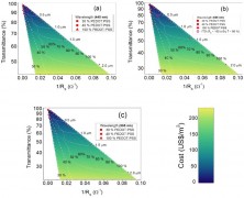
Graphical guidelines: a series of figure of merit charts show the interplay between key performance parameters for different blends and film thicknesses of PEDOT:PSS/PVA (Olivia Carr et al 2015 Transl. Mater. Res. 2 015002).

Graphical guidelines: a series of figure of merit charts show the interplay between key performance parameters for different blends and film thicknesses of PEDOT:PSS/PVA (Olivia Carr et al 2015 Transl. Mater. Res. 2 015002).

Optimizing the composition of the blended film is important to balance the cost versus performance. In many cases, high electrical conductivity and high optical transmittance in the visible range of the electromagnetic spectrum are critical factors. However, other aspects such as flexibility, film formation, chemical stability and wettability can also play an important role in the choice of the material or the composition to be used, together with overall processing considerations.

Case study: semi-transparent electrodes for flexible optoelectronics
In a recent study, published in the journal Translational Materials Research (TMR), materials scientists have examined a blend comprising poly(3,4-ethylenedioxythiophene):polystyrene sulfonate (PEDOT:PSS) and polyvinyl alcohol (PVA), which can be used as a flexible, semi-transparent and highly-conductive material in electronic and optoelectronic devices. The electrical conductivity and optical transmittance of spray-deposited films of various thicknesses and blend ratios were evaluated to determine the most appropriate composition for optimal device performance and cost.

Presenting their results as a series of figure of merit diagrams, the researchers observe that it should be possible to decrease the PEDOT:PSS content in the blend down to 30% (by weight) and maintain an acceptable level of electrical conductivity for many applications.

Full details
Analysis of the electrical and optical properties of PEDOT:PSS/PVA blends for low-cost and high-performance organic electronic and optoelectronic devices
Olivia Carr et al 2015 Transl. Mater. Res. 2 015002

$5 million investment in Angstron Materials accelerates graphene commercialization

Angstron Materials, a US supplier of single and few-layer graphene materials, announced this week that it has secured $5 million in capital to increase manufacturing capacity and bring key technologies such as its thermal management products to market. Heat spreaders developed by the firm can reduce hot-spots in mobile phones and other handheld devices, and the funding news follows reports earlier this year that Angstron’s graphene sheets have been qualified for use by a major mobile electronics company.

Graphene foil

Thermal interface material: Angstron Materials supplies graphene-based sheets in thicknesses ranging from 5 µm to 40 µm with thermal conductivity between 800 W/m.K and 1700 W/m.K for use in electronic products such as tablets, laptops and flat screen TVs. The foils can also be used for EMI shielding.

Estimates by market analyst IDTechEx suggest that 55% of electronic failures are caused by over-heating, and enhanced thermal interface materials have a major role to play in helping devices to stay cool, perform better and last longer as developers boost their offerings by packing more processing power into increasingly compact form-factors.

“We use the planar alignment of carbon atoms to make a lightweight, flexible thermal foil with up to 1700 W/m.K in-plane thermal conductivity – substantially higher thermal conductivity than copper and offering weight savings for thermal management,” Claire Rutiser, a member of Angstron’s executive team, told TMR+. “Also, we can load thermally conductive nano graphene platelets (NGP) into a matrix – which could be thermoset, thermoplastic or non-curing (for thermal paste).”

Graphene isn’t the only option for device makers and competing thermal management materials include formulations based on silver flakes or silver nano-wires, but there are economic considerations that may favour the use of NGPs. “Silver is subject to significant price fluctuation and future price uncertainty,” Rutiser comments. “Angstron Materials has known input materials pricing and is able to enter into long term supply agreements with end users.”

Graphene has been linked with various big names in portable electronics. In 2011, Apple noted that the use of graphene thermal dissipators goes beyond cooling. Related applications include transferring heat from onboard electronics to the battery to improve runtime, which can be compromised at low temperatures.

Multiple markets
Rutiser says that Angstron is ready with scalable production capacity and emphasised that the firm is targeting other sectors in addition to thermal management materials. She’s optimistic that over a 10 year period energy storage will grow to become one of the company’s biggest sources of revenue. Driving this are developments in graphene-wrapped silicon anodes by sister company Nanotek Instruments, which allow fabrication of Li-ion batteries with over 400 Wh/kg, and also materials for supercapacitors.

“Affordable, high-capacity energy storage is critical for the transition to electric vehicles and for grid-stabilization as the percentage of energy derived from renewables increases in the coming decades,” Rutiser explained. “These products have comparatively long qualification times due to reliability testing and industry safety standards.”

Currently, Angstron’s graphene-enhanced products and technologies are linked to five distinct portfolios – thermal management materials, energy storage systems, nanocomposites, transparent conductive films, paints and coatings. “Graphene platelets are inert to most chemical species and offer opportunities to improve barrier coatings against corrosion, chemical attack, or oxygen permeation, “ added Rutiser.

Read next

Thermal interface materials: opportunities and challenges for developers (Rachel Gordon, Translational Materials Research)

Show report: IDTechEx Printed Electronics Europe 2015 (TMR+)

Supercapacitors: market factors to consider (TMR+)

Fullerex talks graphene pricing; identifies growth areas and supply targets (TMR+)

Graphene ‘quilts’ cool down transistors (nanotechweb.org)

Partnerships and revenue models unlock opportunities for smart coatings

In its latest report on emerging technologies, Lux Research has put the spotlight on opportunities for smart coatings. The firm’s analysis highlights the power of partnerships in translating breakthroughs from the lab to the market, which has implications for start-ups in the field of advanced materials. To find out more, TMR+ spoke with Anthony Schiavo, an analyst at Lux Research and lead author of Surfaces Get Smarter: Scouting Emerging Coatings, Markets and Functionalities.

New roles beyond protection
“Today, coatings can do more than just provide protection,” said Schiavo. “They are finding new roles and replacing other components such as inspection systems.” Examples can be found in the US Navy, which has patented a resin that releases a distinct odour when broken. This feature can be exploited to alert crew members to corrosion and mechanical fatigue in out of sight areas of a ship or aircraft.

The Navy system has been designed with the human nose in mind, but there are automated solutions out there too. Another approach involves coating RFID tags with a conductive layer. “When the coating is damaged, the signal will propagate,” explained Schiavo.

Smart materials as a service
The oil and gas sector is another strong prospect for smart coatings, but as Schiavo points out – performance is only part of the picture. Materials suppliers need to pick the right revenue model to ramp up their business.

“Solutions will be more attractive to potential customers if providers can supply advanced materials and coatings as a service rather than a product,” he said. “Suppliers can lower the barrier to entry by tying the value of their products directly to performance, in this case an improvement in downtime figures, rather than attempting to sell tonnes of material outright in advance.”

Cost-benefit analysis
Winners in the consumer electronics segment include firms such as P2i, a provider of chemically bonded hydrophobic coatings, which allow device partners to add-value in highly competitive sectors such as the mobile phone market. “The differentiation you get on a raw technology basis can be very short-lived,” commented Schiavo. “Smart coatings help manufacturers to strengthen the appeal of their products.”

Other exciting firms to watch include LiquiGlide and SLIPS Technologies, which are positioned to impact packaging. Like P2i, their value proposition can be communicated in just a few seconds of video or by a quick product demo, which makes it much easier for these companies to pitch their technology to potential partners.

Read next –

Trajectories in translation: parallels between old and new materials (TMR+)

From protecting soldiers to protecting mobile phones (Stephen Coulson, Translational Materials Research)

Materials inspired by nature (physicsworld.com)