Show report: Metal additive manufacturing 2014 (Sheffield, UK)

As promised in the flyer, the Association of Laser Users (AILU) event brought together a mix of additive manufacturing (AM) experts from industry and academia to discuss the tough topics that are all too often ignored in the media hype surrounding 3D printing. Split into four sessions, the meeting was chaired by Robert Scudamore from manufacturing and fabrication consultants TWI.

Setting the scene
The aerospace sector is a prime candidate for lightweight, lattice structures that are easy to build using AM tools. Also, 3D printers enable a high-level of part customization, which benefits medical implants and patient-specific surgical tools. But both aerospace and medical sectors require significant materials and process qualification.

Also, there are setup costs to factor in. Additive techniques such as 3D printing use much less material than subtractive processes such as milling, but the initial materials outlay can still be high. For example, filling an industrial laser sintering machine with virgin titanium powder can cost thousands of pounds.

Speed of production is another issue, with some parts taking hundreds of hours to build.

Reality check
One of the first speakers to start busting the myths was Robin Wilson from the UK’s Technology Strategy Board (TSB). “Additive manufacturing is not just printing from CAD,” he told delegates. Potential users need to consider the whole process, which as Wilson points out involves a significant “digital data supply chain” and physical “post-processing” of the finished component.

Stéphane Abed of Poly-Shape, who also spoke at the meeting, manufactures parts using a tool path that co-ordinates four beams. These multiple lasers can build several smaller components at once or construct different sections of a single work-piece simultaneously, to improve production rates. But having multiple optical-trains also ramps up the number of variables in the process.

Listening to the presentations, it’s clear that AM has no shortage of parameters that influence the quality of the manufactured part – laser power, writing speed, powder flow rate (for nozzle-blown setups), particle size distribution and recycle rate, are just a few.

It can be done
Throughout the day, process control remained a key talking point. Trevor Illston of Materials Solutions, who led the final session of talks, is optimistic that AM can be controlled to a “production standard” by inspecting workpieces at multiple points in the AM process.

Giving the audience food for thought, Illston added that there can be a downside to the design freedom that 3D printing brings to the table, as it’s possible to create parts that are incredibly difficult to examine!

In general though, unlocking traditional design constraints is a big win for AM – and despite the production challenges, all of the speakers recognized that major opportunities are up for grabs.

The medical sector is a growth area for AM, not just for implants, but also for custom tools such as cutting blocks to guide surgery. Medical centres are looking at options for manufacturing parts in hospital to speed up delivery to the patient. Ideas here include flat-packed production tools that can be sterilized and then assembled in theatre.

“AM often solves one problem beautifully, but it can create other issues,” said Edward Draper of JRI Orthopaedics, who spoke in the opening session. Draper picked up on Wilson’s earlier remark about post-build processing, and emphasised the requirement for cleaning and polishing.

Something new
Images of medical devices, helicopter components and fixtures for satellites are becoming a familiar sight at AM conferences and events, but Neil Burns of Croft Engineering had something new for the audience – filtration parts. Traditionally, Croft Engineering has made filtration supports by shaping wire mesh, but the bending process leads to apertures that are non-uniform. To get around this, Burns showed how his company uses AM (inspired by a trip to Fab Lab in Manchester, UK) to build filtration supports with holes that are aligned to the direction of fluid flow – a design feature that saves customers money by reducing the amount of energy that’s required to pump liquid through the component. Despite the benefits, Burns revealed that clients can be cautious about using AM parts. They fear downtime caused by mechanical failure.

But what is the effect of AM on materials performance? How do AM samples behave under load compared with material that has been cast or milled? AM components might look fine on the outside, but what’s happening to the internal structure of the material? Also, how does the strength of parts made using different machines compare, or parts that are built on the same machine, but formed using a different tool path, or using powders with a different particle size distribution or storage history?

Team effort
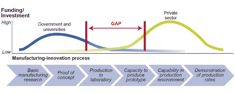
To tackle this, AM needs its own materials database and standards – a point made by many attendees, including Neil Mantle of Rolls-Royce. What’s more, the task requires a collaborative effort. Contributions so far include EU initiatives such as SASAM (Support Action for Standardisation in Additive Manufacturing) and the UK’s ANVIL project to establish benchmarks and design guides for AM.

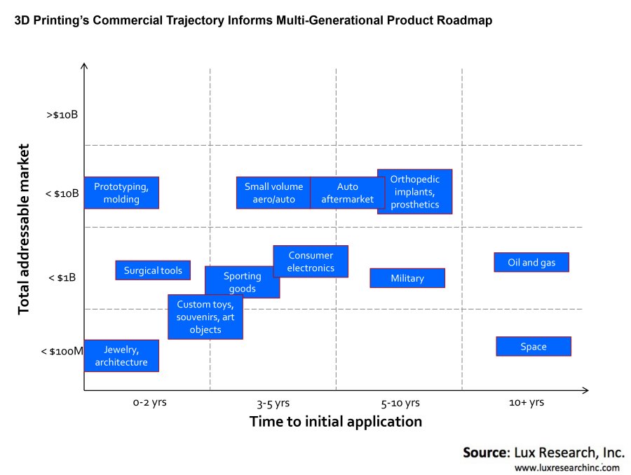
A continuing development is the use of technology hubs to support AM projects at technology readiness levels (TRL) 4-6, or in other words to translate projects from proof-of-concept to pilot-scale operation.

David Wimpenny from the UK’s Manufacturing Technology Centre (MTC), which was established in 2010 to bridge the gap between academia and industry, was at the event. “Our role is to make parts that industry can relate to in terms of size and quality,” he explained.

Today, the MTC is part of the UK’s high value manufacturing (HVM) catapult – a network of seven technology centres with a shared goal of accelerating process innovation.

Related links –

Metal Additive Manufacturing: opportunities in applications and improvements in process technology (full programme)

Supply chain knowledge: formulating and applying new materials

Carbodeon is a supplier of carbon-based additives including detonation produced nanodiamonds (4-6 nm) that offer major upgrades in materials performance, but success in this sector isn’t as straightforward as simply demonstrating record-breaking properties.

“You have to create a situation where delivery is beneficial for everyone in the supply chain otherwise the material won’t make it to the end user,” Gavin Farmer, business development manager at Carbodeon, told TMR+.

Considerations include materials cost, availability and impact on manufacturing.

Nanodiamond is available in dispersions, suspensions and powdered forms (credit: Carbodeon)

Nanodiamond is available in dispersions, suspensions and powdered forms (credit: Carbodeon)


The firm offers chemically-treated nanodiamonds as suspensions (of small agglomerates) and dispersions (of individual particles) that can often be mixed directly with raw materials, and reduce the amount of specialized knowledge required by the customer. Powdered forms are also available, but typically the integration step takes longer to optimize.

For Carbodeon, the split between nanomaterials development and applications-related research is roughly 70/30.

Adoption by industry
The company provides samples of material to clients for assessment, but for this approach to succeed the customer must be willing to enter into a series of experiments and have the tools to validate the results. Also, clients may lack the deep scientific knowledge that could be required to absorb the technology, and require further support.

Where a strong market opportunity exists, Carbodeon will push further into the application area and pursue patent opportunities. This opens the door to licensing revenue and gives added value to the customer through exclusive use rights.

“Whenever you invest in applications-related research, you need to make sure that you can monetize the work,” adds Farmer.

Product development
Success stories for Carbodeon so far include electroplating, where nanodiamonds have been shown to nucleate grains of the coating material, which reduces cracking and ramps up the corrosion protection offered by the electroplated layer. The embedded particles also improve wear and reduce friction thanks to their materials properties.

A notable characteristic of diamond is its very high thermal conductivity, which is rare for materials that are electrically insulating. Carbodeon is working with developers to formulate superior thermal interface material (TIM) and easy-to-process heat sinks for managing cooling in electronics.

“We’ve taken polymers that contain thermal fillers, typically micron-sized boron nitride or alumina particles and milled them with nanodiamond (0.1% by weight),” said Farmer. “The much smaller diamond particles bridge gaps in the filler network to boost thermal conductivity by 25%.”

Driving down emissions
The firm’s latest product is dubbed uDiamond Vox D – a formulation that Carbodeon claims can double surface durability and reduce friction by up to 66 percent.

Pre-functionalized with a surface chemistry tailored to suit PTFE, the liquid dispersion of nanodiamonds can be mixed directly with industrial fluoropolymer coatings ready for application by spray or screen printing with little or no change to the process parameters.

“In automotive powertrains alone, the fuel and CO2 savings through friction reduction will make a real difference,” commented Farmer.

Further reading on the web –

Carbodeon Oy: Better heat conductivity extends equipment lifespan (Tekes)

Materials and equipment upgrades add to 3D printing’s appeal

Back in 2013, TMR+ hinted that the arrival of new feedstocks such as TPU 92A-1 – a flexible and durable thermoplastic – would make 3D printers a much more compelling proposition for product developers. Building on this, there are other factors to consider too –

Commercial additive manufacturing (AM) tools with multiple nozzles are paving the way for 3D-printed workpieces with tailored materials properties – the Objet500 Connex3 is a recent example.

In the lab, researchers are exploring AM designs that combine 3D and ink-jet printing, which bring additional functionality through the use of conductive and other custom inks.

3D printers such as the Freeformer from German production tool maker Arburg further extend the choice of starting materials by accepting granulated feedstock rather than specialized spools of pre-formed material that can turn out to be an expensive option for users.

“The mark-up on feedstock for 3D printing can be anywhere from 10 to 100 times the cost of the raw material, so the Arburg tool could be one way around that,” Anthony Vicari of Lux Research told TMR+. “It’s not just about cheaper materials though, there are other benefits,” he added, “you put your material through one less melt cycle, which should reduce product degradation.”

Vicari and his team have recently updated their projections for high-performance thermoplastics and see additive manufacturing as a growth area for this family of materials as 3D printing migrates from prototyping to manufacturing.

Process improvements are also making an impact.

For example, optics specialist LUXeXcel is using a slow curing technique to upgrade the performance of components printed from transparent resins for use in LEDs and other devices. The approach is designed to combat the formation of stepped features that would otherwise occur as a consequence of layer-by-layer fabrication.

Switching from plastics to ceramics, Vicari mentions Ceralink as another example. The US firm has developed a method for producing silicon carbide/silicon carbide composites using powder bed inkjet 3D printers.

The composite material is said to offer lighter weight, higher temperature performance, and higher wear resistance than nickel alloys and titanium alloys for aerospace jet engine components, and this highlights where 3D printing will have the biggest impact – when it brings something different to the process of translating new materials into devices.

Conventional volume manufacturing techniques such as injection molding will always be cheaper on a per unit basis, but this misses the point of 3D printing.

Commercial outlook

3D printing: applications and market size (click on image to enlarge). Source: Lux Research

3D printing: applications and total addressable market (click on image to enlarge). Source: Lux Research

Some of the unique selling points of AM include customization for market segments such as orthapedic implants, prosthetics and sporting goods. Another positive is product assembly.

“With 3D printing you can often manufacture several parts as one piece, which reduces construction costs, but can also save on regulatory filings too,” Vicari points out.

The on-demand nature of AM means that 3D printing could help firms to reduce product inventory (as well as tooling storage) and lower warehouse costs. It also offers supply-chain security in sectors such as space and defence, by enabling on-site production of replacement parts.

Related links

TPU 92A-1 datasheet (PDF via materialise.com)

Stratasys’ Big Announcement — Multi-colour, Multi-material 3D Printing with the New Objet500 Connex3 (3dprintingindustry.com)

Printing Batteries – new inks and tools allow 3-D printing of lithium-ion technology (MIT Technology review)

3D Printed Silicon Carbide: Ceralink’s Novel Production Process for Jet Engine Material (luxresearchinc.com/blog)

World Economic Forum announces top 10 emerging technologies for 2014

3D printing, self-healing materials and energy-efficient water purification were tagged by the World Economic Forum’s Global Agenda Council on Emerging Technologies as breakthroughs last year, but what does the future look like in 2014? Something that won’t come as a surprise is the key role of advanced materials in driving technology to the next level, as illustrated by our highlights from the 2014 list –

  • Body-adapted Wearable Electronics
  • Small, lightweight and flexible components together with specialized coatings to protect products from sweat and rain. Applications include navigation aids, health monitoring devices and surgical tools.

  • Nanostructured Carbon Composites
  • Lighter, stronger materials for more efficient vehicles, which are easy to recover and reuse.

  • Grid-scale Electricity Storage
  • More affordable alternatives to pumped storage hydropower for overcoming the intermittent nature of clean energy. Concepts being explored include flow-batteries and graphene supercapacitors.

  • Nanowire Lithium-ion Batteries
  • Ramping up battery energy density will extend the range of electric vehicles and increase the running time of mobile devices. Results suggest that designs based on silicon nanowires could deliver 30-40% more electricity than today’s lithium-ion batteries.

  • Brain-computer Interfaces
  • The challenges here build on those of body-adapted wearable electronics to include biocompatible materials and thin film technologies to protect implanted electronics.

Barriers to technology translation
As well as announcing its top 10 emerging technologies for 2014, the council has also voiced its thoughts on major hurdles in the translation pipeline –

“Uninformed public opinion, outdated government and intergovernmental regulations, and inadequate existing funding models for research and development are the greatest challenges in effectively moving new technologies from the research lab to people’s lives.”
Global Agenda Council on Emerging Technologies.

Related stories on the web –

What’s the future for wearable technology? (forumblog.org)

Emerging technology as an agent for change (forumblog.org)

Missing middle in nanomanufacturing hits the headlines

The public release this month of a report on nanomanufacturing by the United States Government Accountability Office (GAO) has stirred up media interest in the “missing middle” by putting the spotlight on an investment gap in manufacturing development that can leave discoveries stranded between the lab and the market.

“The term missing middle has been used to refer to the lack of funding/investment that can occur with respect to manufacturing innovation – that is, maturing manufacturing capabilities and processes to produce technologies at scale.”
GAO-14-181SP Forum on Nanomanufacturing

Funding/Investment Gap in the Manufacturing-Innovation Process. Credit: GAO

Funding/Investment Gap in the Manufacturing-Innovation Process. Credit: GAO


Coverage of the report on the web includes –

Promoting translation
Despite the somewhat downbeat headlines, the report is not all doom and gloom and highlights The NSF Nanosystems Engineering Research Center (NERC) for Nanomanufacturing Systems for Mobile Computing and Mobile Energy Technologies (NASCENT) and The College of Nanoscale Science and Engineering (CNSE) as examples of “ecosystems or infrastructures [that] create the conditions for innovators to more successfully traverse the Valley of Death and the Missing Middle.”

To view a summary of the report and for links to the PDF visit – www.gao.gov/products/GAO-14-181SP

From the lab to the factory floor: financial tools for upscaling production of nanomaterials

A guest post for TMR+ by Tom Eldridge, co-founder of Fullerex

Commodity exchanges have existed for hundreds of years, driving economic growth through efficient and structured marketplaces. The success of these exchanges can be attributed to several key advantages that a market-based system provides participants over other channels of trade, which include – regulatory supervision, trade order and discipline (irrevocable agreements for sale/purchase of goods and materials), access to liquidity, reduction in costs associated with trade, price discovery, the ability to hedge and financing of production through forward sale.

In the market for nanomaterials, despite the considerable promise for various commercial applications, integration by industry has up to now been slow progress. This is due to a range of factors such as uncertainty through health, safety and regulatory issues; lack of agreed material standards; price confusion for buyers; supply insecurity; and often sparse sources of financing for producers.

To address these concerns, the Integrated Nanoscience and Commodity Exchange (INSCX exchange) was established in 2009 through a collaboration between experts in nanoscience and the securities and commodity industry; and in the following year commenced a live marketplace pertaining to nanomaterials.

Since then INSCX exchange, which is a member of the NanoCentral alliance of specialist providers in nanoscience, has driven hitherto non-existent trade interest in nanomaterials and nano-enabled products (such as catalysts, coatings, fertilizers, fuel and oil additives, etc…) by engaging producer/end-user interaction and more importantly by providing nanomaterials producers with the financial tools to be able to respond.

Crossing the funding chasm
Most start-up technology companies experience a funding chasm with few options available between securing initial capital contributions for R&D and moving beyond this stage into commercial production. Upscaling from lab to factory floor is a capital intensive process and at the early stage of business, with little or no revenues, this leaves start-up companies vulnerable to cash flow problems.

Establishing a steady revenue stream often requires high throughput to drive down unit cost and enable businesses to attract large buy orders in the first instance. Producer firms engaging in the exchange’s forward sale mechanism can use this process to manage cash-flow and/or achieve upscale financing.

Rather than relying on external sources of funding such as debt or equity that can be costly and/or dilute ownership, materials producers can use the exchange to mobilise capital from industry and develop their business with sustainable and organic growth.

Small to medium sized enterprises producing and supplying nanomaterials also have the challenge of prioritising development objectives and building successful trade relationships. In a centralised marketplace, these difficulties are more easily overcome since demand for materials is readily accessed and understood (qualified and quantified).

For nanomaterials producers the exchange is not to be regarded as anything other than a mechanism designed to complement the efforts of a producer to win sales, develop new product solutions and to enable essential commercial compliances to be adhered to in trade.

From the perspective of a start-up or early-stage company, benefits of trading on the exchange include:

  • EHS accreditation
  • IP protection
  • Trade insurance
  • Downstream Audit Sequence (DAS) track/trace system
  • Upscale financing facility
  • Trade with existing and/or new customers

Getting to grips with the concept
The exchange system however is not to be confused with a standard distribution agreement (which many nanomaterial producers have found either non-performing and/or expensive in terms of margin), but rather a market system, which generates an income for itself and authorized intermediaries such as Fullerex through trade clearing fees (set at a maximum of 1% of the financial consideration of each trade).

Exchange rules governing agency trade (where a merchant – trade member – of the exchange is acting for a producer or end-user) are bound by the principle of best execution. Over-loading and/or under-cutting of material pricing is strictly prohibited by the exchange. The role of the market system is to broadcast price as instructed.

[Note: Fullerex wishes to make clear that all trade in listed nanomaterials on the INSCX exchange remains for commercial supply and end-use purposes only.]

Show report: NanoEntrepreneurs workshop (London, 28 Jan 2014)

“What does it take to commercialise micro- and nanoscale research and development?” is a tough question to answer in a one-day meeting, but the UK’s NanoKTN managed to pack plenty of advice into the latest in its series of popular NanoEntrepreneurs workshops – held this time in partnership with law firm Covington and Burling (C&B) in London.

The event began by looking at the some of the first steps in the translation pathway from concept to commercialization, which includes tasks such as creating a company and developing an intellectual property (IP) strategy.

IP is a key consideration for any start-up, as the strength of a firm’s IP portfolio is likely to be an important factor in raising funds to grow the business.

In her talk, Morag Peberdy from C&B looked at the different ways a company can protect its ideas, namely – patents, trademarks, copyright, trade secrets and through design registration.

There are some useful questions to ask to identify the most appropriate route to take, for example:

– How easy is it to reverse engineer your product?
– Will you be required to disclose materials details to regularity authorities or via product labelling (a growing concern for developers of nanomaterials)?

It’s not a simple exercise, but there are benefits to thinking about IP sooner rather than later.

“The right strategy will allow you to spend your money wisely and bring savings over the long term,” Peberdy told the audience.

To guide their thoughts, she emphasised the need to focus on the competition – who are they, where are they based, and when will their products hit the market?

In the second half of this introductory session, Peberdy’s colleague James Halstead simplified the starting-out process by distilling the business proposition into a series of key elements –

People (innovators, implementers and investors)
Property (IP and physical property)
Relationships (contacts and contracts)

Like Peberdy, he encouraged firms to begin their strategic thinking early on, in this case to make sure that the interests of innovators, implementers and investors are aligned to head off any future bottlenecks and speed up decision making.

For example, what are the objectives of the company:

– to sell the business,
– out license,
– or to sell technology products and services?

For more details on the workshop, which also included talks on creating trustworthy and dynamic teams, and public support mechanisms for the commercialization of emerging technologies – view the full programme on connect.innovateuk.org.

Trajectories in translation: parallels between old and new materials

Can looking at the commercialization history of mature materials such as Bakelite, Teflon and silicon carbide offer clues to the likely development timelines for today’s rising stars such as graphene, metal organic frameworks, and silver nanowires, to give just a few examples? Analyst firm Lux Research thinks so, and has released its results in a report dubbed “Planning for ripe fruit: Materials innovation lifecycles as a predictive scouting tool.”

In the study, Lux Research looked at the development trajectories of 49 materials by examining the gap from the first major jump in patent activity to the commercialization milestones that followed – a period that typically spanned anywhere from 10 to 25 years, but extended much further in some cases.

From the analysis, the team found that it could group the materials into a number of classes –

whether the material was single- or multi-functional,

whether the discovery was targeted or unplanned,

and whether it was an enhancing or platform technology.

“When we looked at the different materials in each class, we found parallels in the invention-to-commercialization pathways,” Anthony Vicari – one of the lead analysts on the study – told TMR+.

In principle, this means that once you know which category a new material falls into, you can identify some of the likely barriers to commercialization – a framework that could be a big help for start-ups when estimating development times.

“There’s often an unrealistic expectation in how quickly new materials will make it to the market, and this analysis offers a starting point for strategic decision making,” he said.

Different classes, different challenges
Let’s look at some of the development hurdles in more detail, starting with multifunctional materials.

“The big advantage of this class of materials is that they can potentially replace multiple parts, but this typically requires a high level of redesign and significant developer resources, which lengthens the commercialization time,” said Vicari.

“For enhancing materials, it is pretty clear from the beginning what the application is – the challenges here are focused on getting good performance at the right price,” he continued.

Platform technologies on the other hand can pose a deeper problem, as it can take time to figure out what the key applications are.

Vicari gives the example of silicon carbide (SiC). “There was an 80 year gap from demonstration to commercialization,” he points out.

Today, SiC is a key material in LED and power electronics sectors.

Looking at parallels between SiC and emerging materials, Vicari believes that metal-organic frameworks (MOFs), which were first reported in the 1950s, could be on a similar development timeframe. This would see non-niche commercial products launching around 2035.

Further reading on the web –

Metal-organic frameworks for energy storage (Royal Society of Chemistry)

National University of Singapore and BASF team up to develop the use of graphene in organic electronic devices

BASF has formed a partnership with National University of Singapore’s (NUS) Graphene Research Centre (GRC) to develop the use of graphene – a 2D form of carbon – in organic electronic devices, such as organic light emitting diodes (OLED). The goal of the collaboration is to interface graphene films with organic electronic materials to create more efficient and more flexible lighting devices.

“Graphene is a fascinating material, with regard to both its electronic properties and its mechanical strength. We have been engaged in the research of graphene for several years and are now ready to enter partnerships in order to complement and speed up our device development,” commented Josef Wünsch, Senior Vice President of Modeling & Formulation Research at BASF, who is also responsible at the firm for incubation in the area of graphene.

The NUS team at GRC will be responsible for the synthesis and characterisation of the graphene. The researchers have already developed a patent-pending methodology for the reliable growth and transfer of high-quality graphene films onto different flexible substrates that can be used in solar cells and lighting panels.

Translating advanced materials
As Wünsch mentioned, BASF has been exploring potential applications of the so-called “wonder material” for some time. In 2012, the chemicals company opened a Carbon Materials Innovation Center at its Ludwigshafen site in Germany. The center was set up in partnership with the Max Planck Institute for Polymer Research (MPI-P), and the MPI-P and BASF have been jointly researching graphene since 2008.

EC information and networking event on organic electronics scheduled for Feb 2014

The European Commission (EC), together with the Organic Electronics Association and Photonics 21, is organizing an “Information and networking event on organic electronics” to provide information on related calls in the Horizon 2020 ICT LEIT work programme (PDF download).

The event will be held on Friday 14 February 2014 in Brussels (Avenue de Beaulieu 25, Meeting Room 0/S1).

DRAFT Agenda

Continue reading