Focus on innovation: new episodes of NBC Learn update on batteries built using viruses and explore biomedical applications of 3D printing

Science of Innovation – a video series – documents how researchers “imagine, invent, improve and inspire” to deliver solutions in health care, energy storage and transportation, to highlight just a few of the sectors mentioned.

Launched in 2012 to celebrate the 165th birthday of Thomas Edison, the videos are produced by NBC Learn in partnership with the National Science Foundation and the United States Patent and Trademark Office.

New episodes
This month, the team has added six more episodes, including clips on the work of Angela Belcher at MIT, and also featuring Adam Feinberg’s group at Carnegie Mellon University.

Belcher’s use of genetically engineered viruses to grow better batteries is the application that often hits the headlines, but her team is also looking at using the technique to improve solar cells, fuel cells, biofuels and cancer therapies. Feinberg is part of the research community applying 3D printing to solve challenges in healthcare, which includes accelerating drug development and advancing personalized medicine.

Device applications for genetically engineered viruses

Overcoming challenges in 3D bioprinting

More videos in the Science of Innovation series
Other topics featured in the new episodes include the microfabrication of cochlear implants; the use of friction stir welding as a tool for tailoring the strength of metallic components; the application of origami structures to enable the transport and easy deployment of large area devices (such as solar arrays); as well as the development of microcontrollers for virtual reality displays.

Read next
An interview with Gabor Forgacs: from theoretical physics to the business of 3D bio-printing (published in the journal Translational Materials Research)

Open for submissions: TMR focus collection on biomaterials
Guest Editor – Subbu Venkatraman, Nanyang Technological University, Singapore
Since the early days of the artificial hip joint, when metallic, polymeric and even ceramic biomaterials were first implanted as hard-tissue replacements, both natural and synthetic biomaterials have become increasingly important for prolonging as well as improving our quality of life. Building functional body parts from many different material types is now commonplace; transplanting these parts with long-term survivability have become reasonably safe procedures for surgeons. Some of these technologies have progressed so far that the concept of a ‘bionic man’ with several replacement body parts is no longer confined to the world of science fiction [more details].

Related stories
Virus creates nanoelectrode for battery (nanotechweb.org)

Flexible electronics: using laser confocal scanning microscopy to optimize interconnect design

Olympus has released an application note showing how optical metrology can be applied to improve the lifetime and performance of flexible electronics.

The study highlights the work of Dario Gastaldi and his team at the Politecnico di Milano, Italy, who have used laser confocal scanning microscopy to demonstrate how particular interconnect geometries are more resistant to delamination.

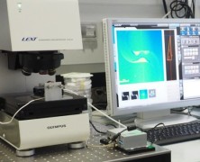
Optimizing interconnect design: micro-tensile testing device coupled to an Olympus laser confocal scanning microscope

Optimizing interconnect design: micro-tensile testing device coupled to a laser confocal scanning microscope

The group’s apparatus features an in-situ micro-tensile testing device coupled to high-resolution imaging equipment (Olympus LEXT OLS4100) and allows the researchers to examine the two main features that have been found to affect adhesion between the interconnect and polymer substrate: geometric parameters and the fabrication process itself.

Design tool
Observing the interconnects under mechanical testing allows the team to focus on key parameters such as strut length and obtain quantitative information, which can be fed back into the design cycle. 3D optical profiles of interconnect geometries allow developers to monitor samples for signs of surface cracking, which can be used to optimize manufacturing processes.

In the work, the researchers observe that plasma treatment of polymers, while increasing adhesion, may promote cracking.

Related links
Lab to market highlights: TMR anniversary collection (free to read)
Flexible and Printed Electronics – a new journal from IOP Publishing

Opportunities for metal mesh, silver nanowires, carbon nanotubes, graphene and other non-ITO transparent conductive films in the touch display industry and elsewhere

The touch panel sector, which has been growing explosively over the past decade, offers tremendous opportunities for new materials and next-generation technologies, but only if developers can accurately grasp market requirements, and identify the sweet spots for their products and services. Jennifer Colegrove, industry analyst and founder of Touch Display Research, has been covering the market in detail since 2006. In this guest post for TMR+, she looks at how the sector has matured, explains why ITO transparent conductive films (TCFs) remain dominant despite their disadvantages and assesses the prospects for new materials.

Overview 2006 – 2020
Touch Display Research forecasts that the touch module revenue will reach $36 billion by 2020, from just $2 billion in 2006.

Figure 1. Touch Module Market Forecast (Image credit: Touch Display Research).

Figure 1. Touch Module Market Forecast (Image credit: Touch Display Research).

Touch screen suppliers, especially those providing projected capacitive touch modules – a popular choice for smart phones and tablets as the technology supports multi-touch gestures – have been mostly profitable during 2007 and 2009. But fast forward to 2016 and the competition is fierce with many touch screen suppliers encountering net losses in recent years as manufacturing capacity has outstripped demand, pushing down panel prices. To become a leader or maintain a leadership position in today’s touch industry, providers need to enhance their offering to customers and introduce new features to drive profits. Continue reading

Mobile World Congress 2016: a big opportunity for graphene

How can 2D materials help mobile device makers and equipment providers to upgrade their core products and grow their business in emerging markets such as wearable technology and the internet of things (IoT)? Visitors at this year’s Mobile World Congress (MWC) will have the chance to find out thanks to the Graphene Pavilion – a live demo space dedicated to 2D materials that makes its debut at the 2016 show (22-25 Feb). Applications on the radar include better batteries and portable power packs, flexible conductive films for touch and other device functions, solutions for network infrastructure, improved sensors and electromagnetic components.

Technology showcase
The Mobile World Congress is the biggest event on the communications industry’s calendar (over 94,000 people visited the show in 2015) and provides a huge opportunity for the graphene community to pitch its breakthrough materials to key customers in the supply chain. At the event, materials providers and leading researchers will be on-hand to discuss how graphene and its derivatives can be integrated into next generation devices and update attendees on the latest scientific results.

Presenters at the Graphene Pavilion include Aixtron, Avanzare, AMO, FlexEnable, GNext, Graphenea, Libre SRL, nVision and Zap&Go, the University of Cambridge, Chalmers University of Technology, the University of Manchester, ICFO – The Institute of Photonic Sciences, Catalan Institute of Nanoscience and Nanotechnology (ICN2), CNR National Research Council and the Italian Institute of Technology.

Lab to market
Recognising that the mobile industry has much to gain from transformative materials, the congress organizers have invited Nobel Laureate Konstantin Novoselov to give a keynote presentation at this year’s event, and scheduled a panel discussion to highlight major opportunities on the horizon.

Links

Graphene Flagship
Mobile World Congress 2016

Read next

Graphene Week 2015: industry opportunities and more (TMR+)
Graphene Pavilion: Day one (Graphene Flagship News)

Software defined sensing: materials developers deploy digital toolkit to access fast-moving markets

Fast-moving opportunities for sensors such as the internet of things (IoT) require a swift approach to translating devices from the lab to the market.

“To move more rapidly and take advantage of the largest growth opportunities in sensors, developers are rethinking the use of new material technologies, and finding places where software can accelerate or even replace steps in the process,” explains Mark Bünger, Vice President of Research at Lux Research, in the latest issue of the journal Translational Materials Research (TMR).

Mark Bünger, Vice President of Research at Lux Research

Mark Bünger, Vice President of Research at Lux Research


Building blocks
Thanks to success of mobile phones and other portable electronics, device-makers have a wealth of sensors such as cameras, microphones and accelerometers to choose from. Pairing these tried and tested components with software can, in many cases, emulate the functionality of much more complex set-ups and provide a swift solution for developers.

Readily available building blocks also include gyros and fingerprint scanners as well as Geiger counters, LIDAR, RFID and FTiR development kits, many of which are supported by online tutorials to aid rapid prototyping.

There are other benefits too, as Bunger points out in the article –
“Off the shelf sensors carry lower technology risk and cost, and the system can be easily upgraded with new software, as we improve our understanding of the phenomena being sensed.”

Markets
Today, software defined sensing is addressing a range of applications, for example –

  • accelerometers can replace heart rate monitors and other devices for fitness/health tracking,
  • depth cameras recognize gestures and can replace touchscreen user-interfaces on consumer electronics,
  • microphones recognize speech and sounds (for example – something burning on stove or the front door opening) for smart home applications.

Full details
To find out more about how device makers and materials designers are fast-tracking the journey from prototype to product, and for an overview of the software defined sensing landscape from a company perspective, read – Accelerating sensor development to the speed of light (Mark Bünger 2015 Transl. Mater. Res. 2 040301).

Related articles

GG_60Before entering the valley of death
Evaluating second-generation attributes is a necessary step in the discovery process explains George Grüner, Editor-In-Chief of the journal Translational Materials Research (TMR)

ON_60An interview with TMR board member Om Nalamasu
Om Nalamasu, CTO of Applied Materials, offers an industrial perspective on managing innovation, and sets the scene for a 21st century of materials

A hype-chart for next-gen batteries: mapping the translation of beyond lithium-ion chemistries from lab to market

Reporting their results in the journal Translational Materials Research, scientists in the US and Germany have monitored research output to assess the prospects for emerging electrical energy storage systems such as Li–air, Li–sulphur and Na–air.

“The reliance of modern electronics and vehicular transportation on rechargeable batteries does not guarantee the acceptance of any new system, even if it is more energy-dense,” caution the authors in their paper. “Cooperation between battery manufacturers and device manufacturers will be important, as will be the creation and support of a dependable supply chain to ensure consistent and sustainable delivery of raw materials of high quality.”

Technology tracking
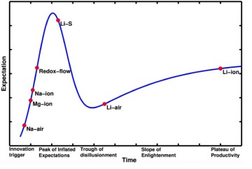
To quantify the status of emerging rechargeable battery technologies, the researchers examined the popularity of each system within the scientific community based on year-by-year publication statistics. From the data, the team was able to identify critical points such as the ‘innovation trigger’ and other characteristic development phases.

Caption goes here

Hype chart derived from publication data showing the status of current and emerging high-energy-density battery systems. A typical technology goes through five phases as it matures and products cycle through different iterations: (i) innovation trigger, (ii) peak of inflated expectations, (iii) trough of disillusionment, (iv) slope of enlightenment and (v) plateau of productivity.

Full details
To find out more about battery design, development and the fundamental materials challenges, view –
Quantifying the promise of ‘beyond’ Li–ion batteries – Oleg Sapunkov et al 2015 Transl. Mater. Res. 2 045002.

Related stories on TMR+

$5 million investment in Angstron Materials accelerates graphene commercialization

TRAM 2015: aerospace industry embraces additive manufacturing

Additive manufacturing (AM) is a major opportunity for materials translation. Layer-by-layer fabrication gives designers the freedom to specify lightweight and highly-integrated components that would be impossible to manufacture using conventional machining or forging techniques. To find out what AM can deliver today and to discuss what’s in the pipeline, TMR+ spoke to presenters at Trends in Advanced Machining, Manufacturing and Materials (TRAM) 2015 – an event supported by Boeing and organized by the UK’s Advanced Manufacturing Research Centre.

For the aerospace industry additive manufacturing is synonymous with powder metallurgy. At the meeting, Robert Smith Graham of Carpenter Technology described the gas atomization technique used by his company to produce powders of alloys based on nickel, iron, cobalt and – in a new venture for the firm – titanium.

Smith Graham stressed the need to define standard metrics for the metallic powders used for aircraft parts, as well as agreed measurement techniques. “The additive manufacturing community has already identified this key issue, and work is already underway with academic institutions, research agencies and other manufacturers to define standard specifications,” he said. “Particle size distribution is one important parameter, and we need to find a consistent way to measure this and other key properties.”

Greg Hyatt of DMG Mori Seiki, a manufacturer of machine tools, highlighted that innovation in laser technology has been crucial for making the technique a viable proposition for aerospace applications. “Commercial laser systems are now capable of producing powers of up to 10 kW,” he said. “This means that we can now deposit kilograms of material per hour rather than grams, which makes the whole process much more cost efficient.”

Hybrid approach
Even so, Hyatt believes that more innovation is need to make additive manufacturing cost-competitive with other metal-processing techniques. He points out that build costs could be reduced significantly by depositing layers onto standard forged parts. “This approach retains the robust mechanical properties of the forged piece, and then additive manufacturing can be used to create fine structures on the part surface. This offers real added value at a much lower cost.”

At the same time, additive manufacturing is becoming more precise, making it possible to tailor the mechanical properties for different areas of the component. “We have case studies where we have deposited materials onto existing parts at rates of more than 10 kg per hour,” said Hyatt. “We have also demonstrated how precise additive manufacturing can yield layers with graded composition.”

Hyatt wasn’t able to share the detail of the case studies, but said that good results have been achieved for a rocket motor nozzle. These components must accelerate a large volume of combustion gases to supersonic velocities within a very short distance, and so must be made from materials that can withstand extreme forces and thermal loading. At the same time, their complex structure requires a number of different machining processes to produce using conventional manufacturing techniques.

According to Hyatt, this highly functional type of part is the current sweet spot for additive manufacturing in the aerospace industry. But, as other talks at the conference revealed, many other applications are waiting in the wings for this truly disruptive technology.

Related stories on TMR+

Arkema emphasises 3D printing in its materials research agenda
Show report: Metal additive manufacturing 2014 (Sheffield, UK)

– Submit your article on additive manufacturing to the journal Translational Materials Research (TMR).

Argonne launches Nano Design Works to support materials commercialization and accelerate the translation of research into products

Argonne National Laboratory has launched Nano Design Works to amplify the impact of its expertise in nanotechnology. Last year, Argonne interacted with more than 600 companies, and hubs such as the Center for Nanoscale Materials offer developers a wealth of scientific knowledge and instrumentation.

Open for business
Dubbed a ‘concierge’ service, Nano Design Works caters for businesses of all sizes to match-make clients with Argonne expertise. “We work with industry partners to solve their enduring R&D challenges, identify commercialization opportunities, license new technologies, and introduce transformational discoveries to the marketplace,” Andreas Roelofs, director of Nano Design Works, told TMR+. “Project scale and duration is flexible, ranging from single-day solutions to multi-year investigations.”

Financing
A variety of funding mechanisms are available for companies to work with Argonne, including securing investment from government agencies and venture capital firms through collaborative proposals. “We think that bringing together the world-class resources of Argonne with the ability of companies to commercialize breakthrough science will be appealing to potential funders,” said Roelofs.

Drugs that use nanotechnology to target only cancerous cells while leaving healthy cells untouched; magnetic nanofibers that could create new, more powerful antennas or be used for novel sensors and dectectors; and nanodiamonds that combine with graphene to create nearly frictionless surfaces, are just a few examples of projects that Nano Design Works is currently engaged in.

Related links

Call for papers: Focus on 2D materials beyond graphene
Which applications are likely to benefit the most from emerging 2D materials and what distinguishing properties are required to enable novel functionalities or novel devices and products?

An interview with board member Peter Littlewood
National labs are well placed to work the middle ground between academia and industry to find solutions to big problems. Peter Littlewood, director of Argonne National Laboratory, talks about his approach to tackling major issues such as energy storage and sustainability.

Infographic: smart materials classified by application and development stage

Lux Research has tracked the translation of smart materials from the lab to the market in its latest report – ‘Get Smart: smart materials as a design paradigm’ – examining advances in the development of smart materials and their adoption by industry.

Smart materials from lab to market: classes, applications and development stages [image credit: Lux Research]

Smart materials from lab to market: classes, applications and development stages – for a larger version of the infographic, click on the image [image credit: Lux Research]

Long incubation times, but rapid commercialization when conditions are right
As you’ll discover by reading TMR+ (most recently in this month’s story on OLEDs) – translating promising results into a robust products can take decades and smart materials are no exception, according to the Lux analysis.

What’s also interesting to note is the rapid pace of commercialization once market conditions are right – pieozelectric materials are a great example. This class of materials was long relegated to niche applications before booming due to adoption in mainstream products such as inkjet printers, digital cameras and smartphones, as Anthony Vicari – lead author of the report – points out.

Related reading on TMR+
Partnerships and revenue models unlock opportunities for smart coatings
Trajectories in translation: parallels between old and new materials

DuPont gearing up for OLED to become display standard

DuPont is scaling up its formulations capability in the area of OLED materials. Recently, the chemicals giant has opened a facility to serve the commercialization of next-generation TVs and other large-format displays. The firm has invested more than $20 million in the plant, which is based at DuPont’s Stine-Haskell Research Center in Delaware, US.

Technology package
Back in June, DuPont announced that it was teaming up with Kateeva, a manufacturer of industrial ink-jet printing equipment, to optimize materials and processes to advance the fabrication of Organic Light Emitting Diode (OLED) displays.

Printed displays give developers the opportunity to reduce material waste compared with evaporative techniques and target more competitive price-points for their products.

Applications for OLED materials also include lighting, and DuPont is working with the Holst Centre on this topic as part of an extended collaboration reported in 2014.

Timeline
DuPont has been building its portfolio of OLED materials for 15 years. In 2000, the firm acquired UNIAX – a pioneering display company founded by Alan Heeger, which was spun out of the University of California, Santa Barbara (UCSB) in 1990. Heeger is a winner of the 2000 Nobel Prize in chemistry (together with Alan G. MacDiarmid and Hideki Shirakawa) for the discovery and development of electrically conducting polymers.

Related stories on TMR+
How can you reduce the cost of flexible electronics?

Related articles from the journal Translational Materials Research (TMR)
Organic electronics: Europe builds TOLAE portfolio to address markets (Transl. Mater. Res. 2 030302)
An interview with board member Serdar Sariciftci (Transl. Mater. Res. 2 010202)
Singlet harvesting copper-based emitters: a modular approach towards next-generation OLED technology (Transl. Mater. Res. 1 015003)