As Europe’s Graphene Flagship enters its third year, we highlight how the programme is supporting the commercialization of 2D materials through Graphene Connect – a series of interactive workshops that bring industry and academia together.
“I think the Graphene Connect workshop we attended was a great opportunity to measure the pulse on the applications,” said Amer Ali, CEO of Graphensic AB – a Swedish company producing graphene on silicon carbide. “At the event, we got in touch with skilled researchers and industry incumbents who were genuinely interested in what we do.”
Biomedical briefing
Kostas Kostarelos, who leads the Nanomedicine Lab at the University of Manchester, UK, was a keynote speaker at Graphene Connect’s most recent workshop, which took place in February and showcased opportunities for 2D materials in biomedical technology. “The workshops are so important because they help to give companies a better understanding of graphene and how it can shape their roadmap going forward,” he explained.
More workshops planned for 2016: the organizing team is in the process of finalizing the next graphene connect event and will be announcing full details shortly on their website.
Applications discussed at the February workshop included smart clothes, sensor systems, wearables, packaging, electrodes and other ways that graphene can be used within the body. The events also provide the opportunity for a wider conversation on 2D materials.
“I wanted to understand more about the ‘translational potential’ and associated risk of graphene as well as the medical applications,” added Daniel Chew, Director of Neural Interfaces for GlaxoSmithKline. “Attending Graphene Connect helped to answer a lot of my questions and it was really good to see a wide interest in graphene from different industry sectors.”
Hot topics
The first Graphene Connect event took place in 2014, as part of Graphene Week, and themes covered so far by the workshop series include – nanocomposites, sensors, energy, optoelectronics and photonics, materials and production, investment opportunities and, as mentioned above, biomedical technology.
Additive manufacturing (AM) is a major opportunity for materials translation. Layer-by-layer fabrication gives designers the freedom to specify lightweight and highly-integrated components that would be impossible to manufacture using conventional machining or forging techniques. To find out what AM can deliver today and to discuss what’s in the pipeline, TMR+ spoke to presenters at Trends in Advanced Machining, Manufacturing and Materials (TRAM) 2015 – an event supported by Boeing and organized by the UK’s Advanced Manufacturing Research Centre.
For the aerospace industry additive manufacturing is synonymous with powder metallurgy. At the meeting, Robert Smith Graham of Carpenter Technology described the gas atomization technique used by his company to produce powders of alloys based on nickel, iron, cobalt and – in a new venture for the firm – titanium.
Smith Graham stressed the need to define standard metrics for the metallic powders used for aircraft parts, as well as agreed measurement techniques. “The additive manufacturing community has already identified this key issue, and work is already underway with academic institutions, research agencies and other manufacturers to define standard specifications,” he said. “Particle size distribution is one important parameter, and we need to find a consistent way to measure this and other key properties.”
Greg Hyatt of DMG Mori Seiki, a manufacturer of machine tools, highlighted that innovation in laser technology has been crucial for making the technique a viable proposition for aerospace applications. “Commercial laser systems are now capable of producing powers of up to 10 kW,” he said. “This means that we can now deposit kilograms of material per hour rather than grams, which makes the whole process much more cost efficient.”
Hybrid approach
Even so, Hyatt believes that more innovation is need to make additive manufacturing cost-competitive with other metal-processing techniques. He points out that build costs could be reduced significantly by depositing layers onto standard forged parts. “This approach retains the robust mechanical properties of the forged piece, and then additive manufacturing can be used to create fine structures on the part surface. This offers real added value at a much lower cost.”
At the same time, additive manufacturing is becoming more precise, making it possible to tailor the mechanical properties for different areas of the component. “We have case studies where we have deposited materials onto existing parts at rates of more than 10 kg per hour,” said Hyatt. “We have also demonstrated how precise additive manufacturing can yield layers with graded composition.”
Hyatt wasn’t able to share the detail of the case studies, but said that good results have been achieved for a rocket motor nozzle. These components must accelerate a large volume of combustion gases to supersonic velocities within a very short distance, and so must be made from materials that can withstand extreme forces and thermal loading. At the same time, their complex structure requires a number of different machining processes to produce using conventional manufacturing techniques.
According to Hyatt, this highly functional type of part is the current sweet spot for additive manufacturing in the aerospace industry. But, as other talks at the conference revealed, many other applications are waiting in the wings for this truly disruptive technology.
The UK welcomed an influx of graphene experts last week as Manchester University’s 200+ researchers working in the field of 2D materials were joined by hundreds more for Graphene Week 2015. The event, now in its 10th year, has grown from a small European workshop into a five-day conference boasting over 600 attendees and pushing the University Place venue to capacity. The scope of the programme has expanded too; hexagonal boron nitride (hBN), molybdenum disulphide (MoS2) and other related 2D materials have joined graphene on the ‘menu’ of structures being explored by developers. Most recently, the conference has been co-ordinated by the Graphene Flagship – a European drive to capitalize on the many opportunities for 2D materials, which launched in October 2013 and has adopted Graphene Week as its annual conference.
Plenary update: Nobel Prize winner Kostya Novoselov briefed the Graphene Week 2015 audience on major developments in the field of 2D materials.
The European Commission (EC) has given graphene and related 2D materials research a huge boost through its Flagship initiative, but as Thomas Skordas, head of the EC’s FET Flagships Unit, reminded the audience during the conference opening – the funding is not a blank cheque for 10 years. The objective is to deliver economic benefits. So far, Graphene Flagship projects have generated 3x more publications compared with the Horizon 2020 average, but to achieve its long term goal the programme needs to capitalize on this research growth.
Connecting with industry
The challenge of taking graphene and related 2D materials from the lab to the market is a focus issue for TMR+ and its sister journal Translational Materials Research (TMR), and we were delighted to be invited to the Flagship’s latest Graphene Connect workshop, co-located with Graphene Week 2015, to join in the discussion.
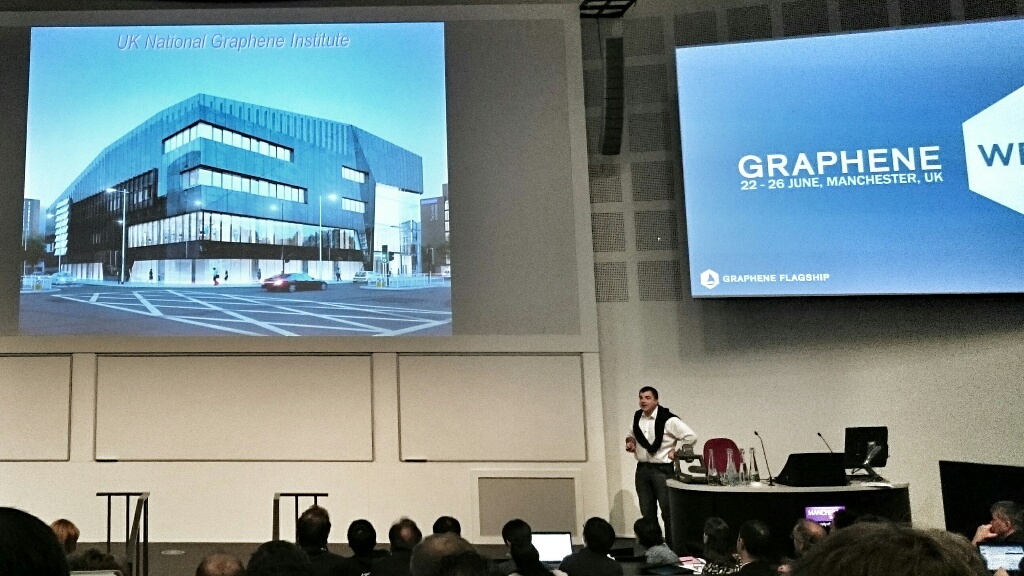
New facility: the Graphene Connect networking event focusing on investment opportunities was held at the UK’s National Graphene Institute in Manchester.
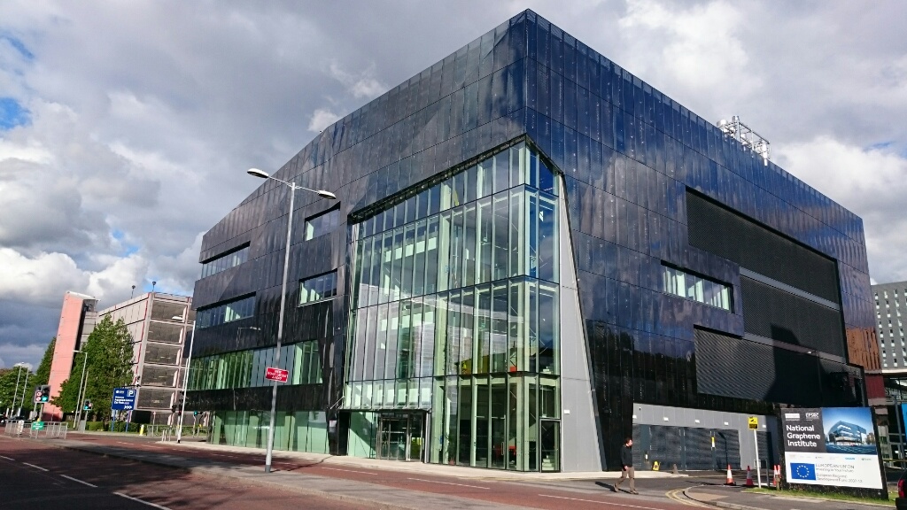
The Manchester session was focused on investment opportunities in graphene and related 2D materials, and put the spotlight on start-ups and early-stage companies. Fittingly, the workshop took place at the recently opened National Graphene Institute (NGI) – a facility where academia and industry are co-located to promote translation of 2D materials from the lab to the market.
Presenters from the VC community included Achim Hoffman of IP Group. He picked up on the issue of media hype surrounding graphene, which has distorted expectations. One of the key messages from the session was the need to stay focused on the fundamentals such as the market, the technology and the infrastructure. “You’ve got to go back to basics,” summed up MTI’s Mark Rahn, who also spoke at the event.
Rahn presented a snapshot of companies operating in the graphene sector. Today, materials suppliers are putting resource into stepping up the value chain by offering functionalized products and formulations that are easier for customers to evaluate and integrate. “The real hard work is how you get from a good idea to a viable production process,” said Nigel Salter, Managing Director of 2DTech – a start-up supplying graphene nanoplatelets (GNPs).
Other industrial players at the workshop included BGT Materials, a 2D materials venture with a base in the UK and a sister operation in Taiwan. According to its UK manager – Liam Britnell – BGT has developed an environmentally-friendly way to process graphene-oxide (GO). Applications include barrier films for food packaging, which exploits the material’s very low oxygen transmission characteristics.
Hexagonal highlights: the National Graphene Institute’s carbon-black coloured cladding is patterned with graphene-shaped perforations.
Whether it’s packaging or microelectronics, materials firms need to understand their potential markets and make sure that their products and processes are compatible with their target industries. To accelerate this process, Applied Nanolayers (ANL) – which grew out of Leiden University – decided to break the cord from academia early on and moved south to base itself in the heart of the Netherlands’ chip-making ecosystem. The company provides wafer-grown 2D material such as graphene or hBN for a range of device applications.
Business briefing
The final panel discussion of the day, which featured Graphenea, Haydale and Flexenable, highlighted the many different routes for growing and repositioning businesses in the advanced materials sector – topics that TMR will be exploring in more detail through its journal section ‘Policy, funding and business strategy’.
Graphenea began as a supplier of 2D materials for the research community, but the firm’s products also appeal to industry and in 2013 it won investment from Repsol – a multinational with activities upstream and downstream in the oil & gas sector. Most recently, Graphenea has been awarded Euro 2.5 million through the Horizon 2020 SME instrument – a phased programme of support to small-to-medium enterprises – which will allow the San Sebastian headquartered company to further scale-up its production capacity. The firm has a satellite office based in Boston, US, to strengthen its links with MIT and Harvard.
Haydale has raised capital by floating on the London Stock Exchange, and recently acquired EPL Composites, which gives the firm an immediate route into this applications area. Haydale has built a strong case for the benefits of graphene functionalization through independent testing of its materials by the UK’s national measurement institute – NPL.
FlexEnable was spun out of Plastic Logic to give the business more freedom to apply its expertise in printing transistors on plastic beyond the display sector. Its activities include consulting services to materials companies.
Meanwhile, back at Graphene Week
There was plenty of industry input at the main conference too with updates from Bosch, IBM and Alcatel Lucent, to name just a few of the big names eyeing up opportunities for 2D materials. TMR+ spoke with IBM’s Shu-Jen Han last year, and the message remains the same in 2015 – RF devices rather than digital logic are a stronger proposition for graphene. Telecomms could be a promising area for the material thanks to graphene’s consistent performance across a wide temperature range, and useful optical properties.
Smart space: The National Graphene Institute features a ‘high-rise wildflower meadow’ designed to improve roof function by providing a green space for people and pollinators such as bees, butterflies and hoverflies. For a video tour of the building, including the lab space, check out the YouTube clip from TMR+’s sister site physicsworld.com.
Alcatel Lucent has been working with partner AMO Aachen to investigate the potential of 2D materials in enabling highly-integrated photonic subsystems. The team has come up with a photodetector featuring CVD-grown graphene on a Si waveguide, which operates in the c-band (wavelength = 1550 nm) to support data rates up to 50 GBit/s.
The next Graphene Connect workshop is scheduled for early 2016 and will explore the topic of biosensors and implants. Graphene Week 2016 will take place in Poland next June.
IDTechEx’s multi-track conference and exhibition explores the interconnected landscape of printed electronics, wearable technology, energy harvesting, the internet of things (IoT), graphene and 2D materials, 3D printing, and electric vehicles. Collaboration is key to succeeding in materials translation, and for me this was one of the big messages of the 2015 show, which brings together formulation specialists, systems developers, fabrication experts, measurement providers, and customer groups, all under the same roof for two days (or more if you sign-up to masterclasses).
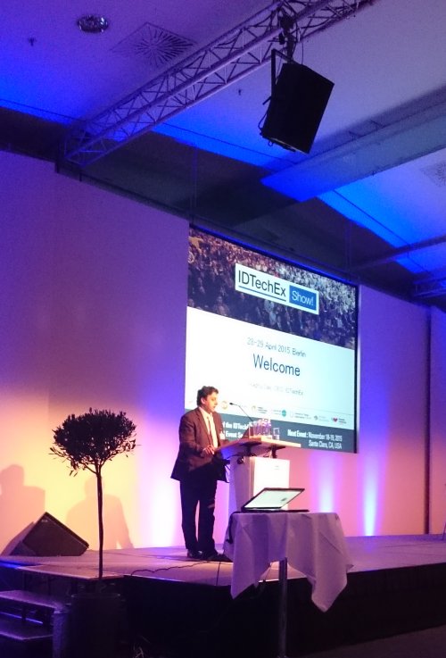
Keynote welcome: Raghu Das, CEO of IDTechEx, briefs the audience on market projections for the printed electronics sector.
Dialogue between technology providers and end-users helps to resolve uncertainty in emerging fields such as printed and flexible electronics where – i) customers can be unsure about what’s possible and ii) suppliers need guidance on market requirements.
Bringing new technology to market
On day one, speakers from Qualcomm and Flextronics outlined how their firms bring new technology to the market. In Qualcomm’s case, its approach is built on four pillars – i) system R&D leadership, ii) design for manufacturability, iii) supply chain management and iv) customer support and engineering. It’s important not to overlook the final step. “The value proposition is only realized if you can propagate this to the customer,” Stein Lundby (R&D manager at Qualcomm) reiterated to audience.
Qualcomm, which Lundby describes as a ‘surface electronics’ company, is exploring opportunities for a hybrid product combining traditional crystalline based electronics with printed electronic components. Developed with Enfucell – a provider of printed power sources – the device features a 3-axis gyroscope and 3-axis accelerometer together with integrated battery and system electronics packaged in a band-aid style form factor. Users can stick the sensor on items such as golf clubs to determine how new products might improve their game, but this is just one possible scenario.
To navigate markets such as wearables, Flextronics – which focuses on production equipment and know-how – has opened design centres to help customers with product development and new use-cases such as electronic displays for athletic clothing. In his presentation, Keith Churches (head of innovation services at Flextronics) showed how the company brings new ideas to the market by configuring product-specific development networks that link the firm’s expertise with partners such as OEMs, universities and research institutes.
Nanomaterials Directa Plus – which was founded in 2005 and opened its graphene factory in 2014 – used the graphene and 2D materials conference track to talk through its collaboration with Vittoria Industries and highlight early market opportunities for graphene. Dubbed the wonder material, graphene – an ultra-thin layer of carbon – has been shown to have record-breaking electrical, thermal and mechanical properties, but breakthrough results in the lab don’t guarantee commercial success. “You have to be brave to be in the graphene market,” Giulio Cesareo (CEO of Directa Plus) commented.
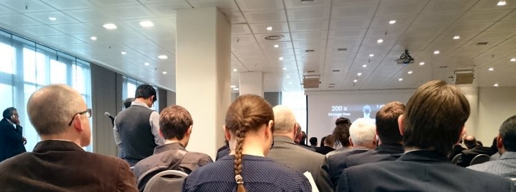
Full house: interest in graphene and related 2D materials remains strong.
Vittoria uses Directa Plus’ graphene nanoplatelets to formulate bicycle tyres and wheels with enhanced properties such as heat dissipation and lateral stiffness. There are 165 wheel makers in the world, Rudi Campagne (founder of Vittoria Industries) told the audience, and the use of nanomaterials such as graphene is an effective way for Vittoria to differentiate itself from the competition.
Early uses of graphene provide a platform for growth in other sectors by establishing a materials supply chain. Beyond tyres and wheels, Directa Plus is looking at opportunities for graphene in cleaning up contaminated soil and water. In his talk, Cesareo explained that linked graphene platelets have the potential to remove hydrocarbon pollution from lakes, according to test results. Literature from the firm claims that 1 gram of its Graphene Plus sorbent can adsorb up to 80-90 grams of oil – for more details, visit the GEnIuS project website, a programme co-founded by European Union within the Eco-Innovation initiative.
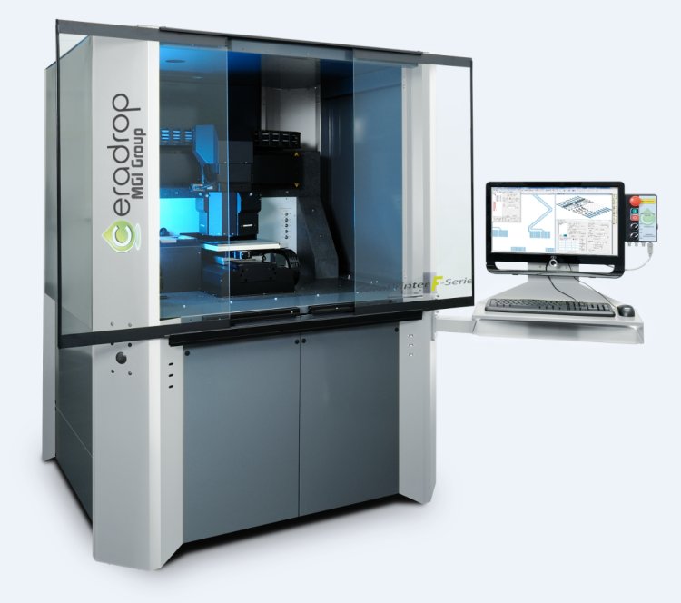
Exhibition: new products launched at the show included Ceradrop’s ‘F-Serie’ multi-material printer.
The discussion then moved on to opportunities for 2D materials in the electronics industry. If graphene does make an impact in this sector it is likely to be driven by novel applications, based on the views of the speakers in the opening session. “Graphene will not replace silicon in standard devices,” commented Guenther Ruhl (lead principal in new materials at Infineon Technologies) during his talk.
Touch screens are also looking unlikely as a big opportunity for graphene. “Graphene transparent conductive films are among the worst performers in a crowded market,” explained Khasha Ghaffarzadeh (head of consulting at IDTechEx). Like Ruhl, he feels that 2D materials could have more impact in new product categories. “The beauty of graphene is that there are many target industries and applications,” Ghaffarzadeh added.
OPV and R2R technology
Analyst events such as the IDTechEx show give attendees a view on tomorrow’s technology today. Two further highlights for me from the keynote presentations were Heliatek’s building integrated photovoltaics (BIPV) and Asahi Kasei’s e-beam fabricated seamless roller for printing transistors.
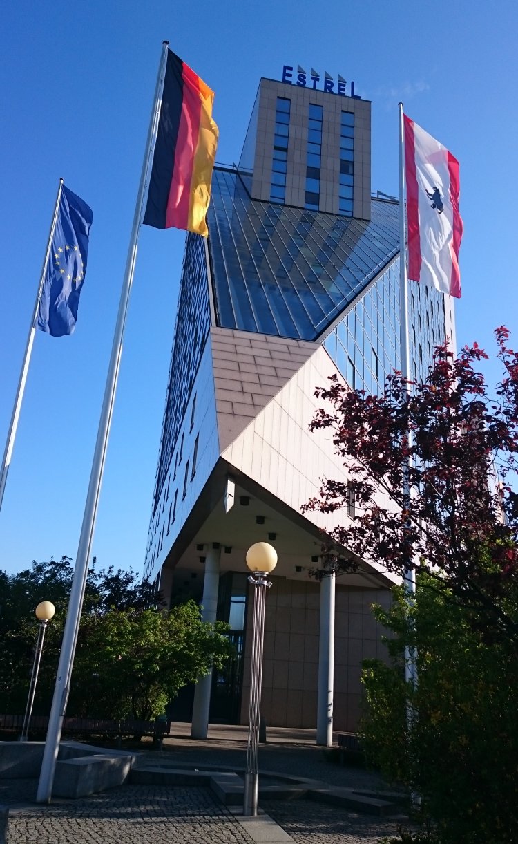
Show venue: Estrel, Berlin
In the afternoon on day one, Martin Pfeiffer (chief technology officer at Heliatek) outlined what he feels is a sweet spot for OPV – active facades. To compete with silicon, OPV has to bring something different, which it can when applications demand flexible and lightweight solutions. He added that the energy payback for an OPV cell can be as little as 3 months, as determined by the EU project dubbed X10D. Pfeiffer revealed that large-scale trials of the firm’s material were now underway in China and Germany on concrete (in Shanghai), PVC membrane (in Berlin) and glass (in Dresden) structures, with another pilot project due to start soon in Singapore on a glass and steel construction.
There were more glimpses of the future on day two when Masayuki Abe of Japanese giant Asahi Kasei – which operates in chemicals, electronics and healthcare sectors – presented his team’s work on seamless roller mold (SRM) technology for roll-to-roll (R2R) printing of sub-micron feature sizes. To make the mold, they rotated a super-smooth (2 nm roughness) roller under an e-beam writer. Moving the roller laterally (as well as rotating it) allows the team to create complex mold patterns. To test the process, Abe’s group used one of its roller molds to print a 200 ppi, 125 micron pitch TFT array. Abe was clearly proud of his team’s results and sees a bright future for the technique. “SRM will bring about the realization of high-resolution printing,” he told the audience.
Dates for your diary
The IDTechEx conference and exhibition takes place twice annually – once in Europe and once in the US (18-19 Nov 2015). The event returns to Berlin on the 27th and 28th of April 2016.
Europe’s Graphene Flagship has released details of its 6th Graphene Connect workshop, which aims to introduce business angels to graphene and create an arena for small to medium enterprises (SMEs) and venture capital (VC) firms to interact.
‘The purpose of the flagship is not to perform research — it’s to bring research into society,’ Helena Theander, a senior member of the Graphene Flagship’s innovation team, told Translational Materials Research (TMR) in a recent article highlighting the need to engage SMEs in materials commercialization. ‘Graphene Connect is a process to get more industry players interested in graphene and related 2D materials.’
This latest installment in the Graphene Connect series coincides with Graphene Week 2015 and will take place in Manchester, UK, on Monday 22 June.
The workshop programme includes –
Presentations by firms operating in the graphene sector.
VC talks on investing in graphene given by industry representatives, followed by a panel discussion.
Matchmaking activities for SMEs and entrepreneurs to meet and interact with the venture capital community and explore business opportunities.
To register for the workshop, visit the event website.
MATERIALICA has been championing new materials and innovative applications since launching its awards program in 2003. “We honour products which combine outstanding design and high technology expertise,” explained Robert Metzger, jury member and organizer of the MATERIALICA Design + Technology Award.
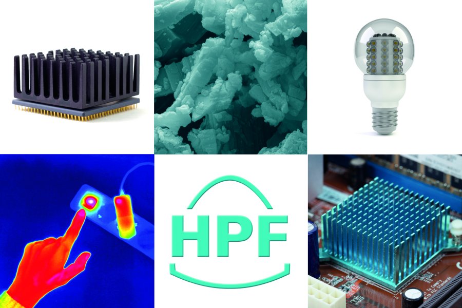
Last year‘s winners include Budenheim’s Excelion material, which is used to advance lithium ion batteries, and SILATHERM from HPF, which improves the thermal conductivity of plastics without downgrading the electrically insulating properties of the host substance. Also recognised in 2014 were LZN Laser Zentrum Nord and EDAG Engineering – co-recipients of the silver award for surface technology. The prize acknowledges the winners’ use of 3D printing to enable a multifunctional aluminium housing for electric vehicles, which weighs just 900 g compared with 1900 g for the reference casting.
In 2013, I-MEET (Institute of Materials for Electronics and Energy Technology, University Erlangen-Nuremberg) won the gold product award for its solution-processed flexible semitransparent organic solar cells. The modules are laser patterned and feature silver nanowire meshes as top and bottom electrodes. Applications for the devices include windows (the cells exhibit 56% transmittance at 550 nm) and skylights.
The deadline for submitting nominations to the selection committee is 17 July 2015. Application forms and further details can be found by visiting materialica.com
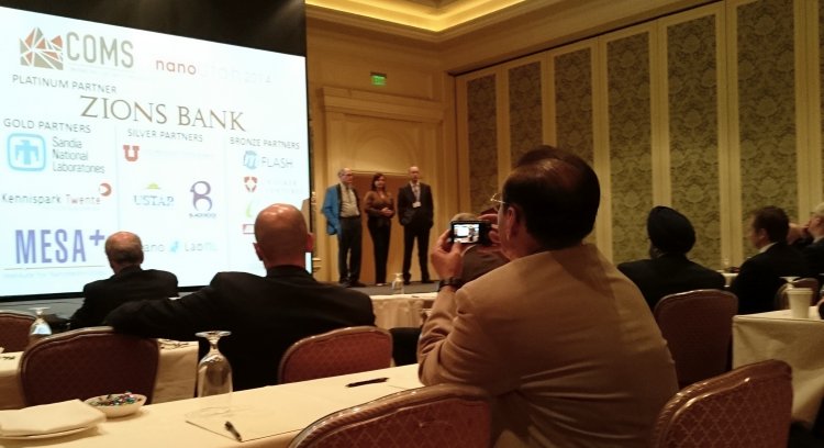
Through its flagship COMS event, MANCEF brings together academia and industry to promote the commercialization of micro-, nano- and emerging technologies, and encourage entrepreneurship. This year, the conference was hosted and co-organized by the Center for Engineering Innovation at the University of Utah. In his welcome address, Tom Parks, vice president for research, emphasized that spin-outs are a key part of the university landscape. “Enterpreneurship offers career development for faculty and students,” he explained. “It’s not just about the money, there are longer term benefits.”
Opening remarks: Steve Walsh (University of New Mexico), Florian Solzbacher (University of Utah) and Maggie Janat-Amsbury (nanoUtah) welcome attendees to COMS 2014
Talking venture capital
As regular attendees to the conference will know, COMS is a practical meeting featuring a mix of talks and Q&A events designed to explore the process of taking a product to market, finding new customers and identifying development partners. Highlights on day one included the investor and venture capital panel discussion chaired by David Blivin of Cottonwood Technology Fund. In the session, funders described what they look for in a start-up and panel members included James Smith, who helped run the CIA’s venture fund dubbed In-Q-Tel.
Smith likes to see start-ups with a clear product definition and a data sheet to go with it. He’s encouraged when founders know who their customers are and have orders on the horizon, which reduces the risk for investors. Even with these points ticked off, uncertainty remains in the ability of an early-stage company to deliver. The panel agreed that a start-up’s technology lead needs to be aware of the different skill sets required for the journey beyond the lab. “It’s unlikely that a founder will take a company from cradle to grave,” commented Todd Stevens of Renewable Tech Ventures, who also sat on the panel. Like many investors he looks not just at the technology, but also at the people leading the project. “Market conditions may change and the management team needs to be able to adapt,” Stevens told the audience. Smith added that it’s important for founders to be self-aware and know their limitations. As the panel highlighted, one way for a firm to expand its expertise is by forming strategic partnerships to help with tasks such as manufacturing scale up and distribution.
Supporting technology translation: Deborah Jackson of the National Science Foundation (NSF)
Promoting innovation
Spurred on by the theme of the morning plenary session on day two – The new age of materials: why translation matters – given by George Grüner of UCLA, attendees gathered after lunch for the sequel event chaired by the journal Translational Materials Research (TMR). Deborah Jackson of the National Science Foundation (NSF) spoke first on sizing up your innovation ecosystem and pinpointing strengths and weaknesses so that appropriate support can be provided. “We don’t try to apply the silicon valley model across the board,” she explained.
Joining Jackson on the programme were Fiona Jamieson of the Institute of Physics (IOP), who presented key findings on graphene commercialization in the UK and Europe, and Deb Newberry of Nano-Link, who updated on progress being made in upskilling workers for careers involving nanotechnology. To close the popular session, Xiao Zhang of Hitachi High Tehnologies, reported his team’s work on upgrading TEM apparatus to operate under industrially relevant conditions, which he hopes will accelerate the translation of materials discoveries into robust products and devices.
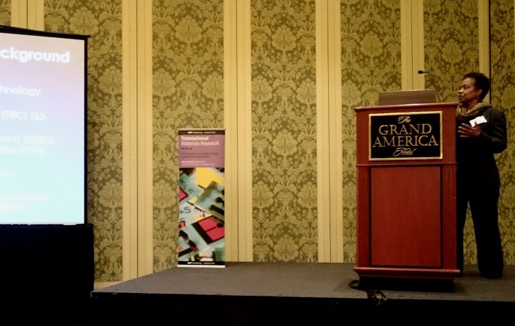
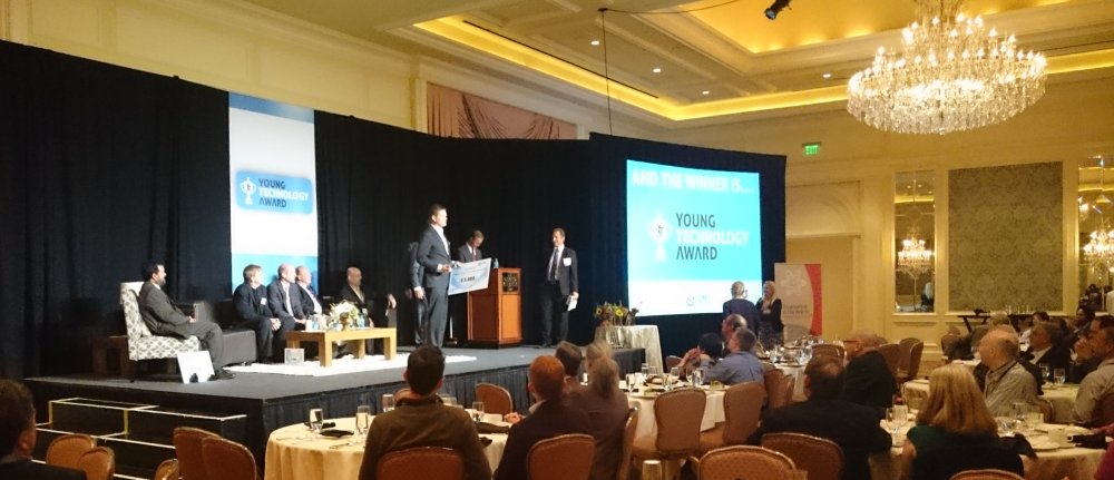
Prize-winning technology: Bernd Vinke of Tide Microfluidics receives both audience and judges prizes at the 2014 Young Technology Award.
Show time
Evening entertainment at COMS includes the Young Technology Award where attendees get to vote on a series of 3 minute pitches given by entrepreneurs attending the conference. This year, the audience and the judging panel were in agreement as Dutch start-up Tide Microfluidics, which has developed a platform for producing highly monodisperse microbubbles for applications in medical imaging and drug delivery, won both prizes and grabbed valuable media attention along the way (see news links and tweets below).
For more information on COMS and for announcements on the 2015 event, visit the MANCEF website.
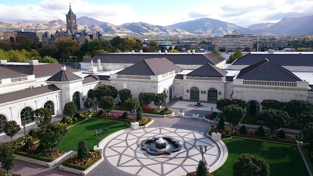
Venue with a view: Grand America hotel and conference facility, Salt Lake City, Utah, US
TMR+ is in Utah this week for COMS 2014 – a key conference on the lab-to-market events calendar looking at the commercialization of micro, nano and emerging technologies. The four day meeting, which was held in Europe last year, focuses primarily on entrepreneurship and marketable solutions, not just science and technology. And with its Young Technology Award and accompanying bootcamp session for entrants, the event takes a hands on and practical approach to guiding entrepreneurs from university spin-outs and early-stage companies.
The conference features lab and company visits, and a series of plenary sessions examining the commercialization process from first idea to final product. Keynote speakers at this year’s meeting include George Gruner of UCLA, who will be commenting on the search for application-relevant materials and changes in the research landscape.
Building on these themes, Translational Materials Research (TMR) is chairing a session – The New Age of Materials: Why Translation Matters (Track C4) – featuring Deborah Jackson from the National Science Foundation (NSF), Fiona Jamieson – science and innovation officer at the Institute of Physics (IOP), Deborah Newbury from the Nano-Link Center, and Xiao Feng Zhang of Hitachi High Technologies.
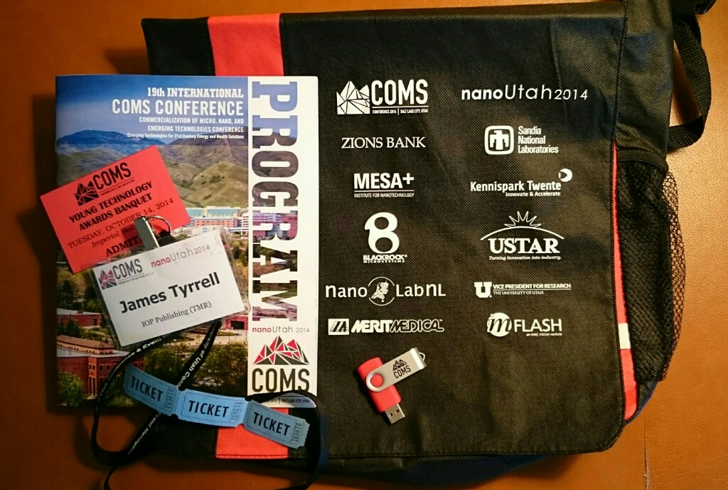
Registered and ready to go: TMR+ will be posting highlights from COMS 2014
The full COMS 2014 programme is available online and I’d encourage you to come along to the conference if you’re in the area on Monday 13th, Tuesday 14th or Wednesday 15th of October.
Show report
If you’re unable to attend, but still want to follow the meeting then register for updates on TMR+ as we’ll be posting a show report for COMS 2014. It’s easy to sign up, just look for the “subscribe to email alerts” box on TMR+.
MANCEF’s commercialization of micro, nano, and emerging technologies conference (COMS) gives early-stage companies in these fields the opportunity for expert feedback through its Young Technology Award.
Sunday 12 October 2014, noon to 7 pm – expert bootcamp and pitch training
Tuesday 14 October 2014, from 6:30 pm – top six entrants go through to the Young Technology Award final held at the Natural history museum of Utah.
Focus on materials translation
Other highlights in the COMS 2014 program include a session chaired by the journal Translational Materials Research (Track C4 – Tuesday 14 October, 2 pm) looking at progress in the commercialization of devices based on graphene, and exploring the acceleration of materials translation through innovation ecosystems.
Graphene Week is now the annual showcase event for Europe’s Graphene Flagship programme – a 10 year, Euro 1 billion initiative that hopes to accelerate the translation of the so-called wonder material from lab to market. For attendees, the five-day conference is a chance to find out what big names in the field such as Nobel-prize-winner Andre Geim think about graphene’s prospects.
As Geim observes in the clip, currently applications are focused on using graphene as a substitute to other materials. But what he’s really looking forward to are applications unique to graphene – uses where the 2D allotrope of carbon performs a function that no other material can achieve.
Other experts at the event included leaders of the Flagship’s 16 work packages (WPs). Andrea Ferrari (WP 5 – Optoelectronics), who’s based at the Cambridge Graphene Center, sees graphene’s optical properties as beneficial for shaping laser pulses and creating photodetectors that operate in the infrared.
Joining Ferrari on WP 5 is Frank Koppens – group leader at ICFO in Barcelona. Koppens is already talking about building prototypes and taking devices out of the lab to demonstrate the industrial relevance of graphene in areas such as automotive night vision.