The touch panel sector, which has been growing explosively over the past decade, offers tremendous opportunities for new materials and next-generation technologies, but only if developers can accurately grasp market requirements, and identify the sweet spots for their products and services. Jennifer Colegrove, industry analyst and founder of Touch Display Research, has been covering the market in detail since 2006. In this guest post for TMR+, she looks at how the sector has matured, explains why ITO transparent conductive films (TCFs) remain dominant despite their disadvantages and assesses the prospects for new materials.
Overview 2006 – 2020
Touch Display Research forecasts that the touch module revenue will reach $36 billion by 2020, from just $2 billion in 2006.
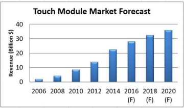
Figure 1. Touch Module Market Forecast (Image credit: Touch Display Research).
Touch screen suppliers, especially those providing projected capacitive touch modules – a popular choice for smart phones and tablets as the technology supports multi-touch gestures – have been mostly profitable during 2007 and 2009. But fast forward to 2016 and the competition is fierce with many touch screen suppliers encountering net losses in recent years as manufacturing capacity has outstripped demand, pushing down panel prices. To become a leader or maintain a leadership position in today’s touch industry, providers need to enhance their offering to customers and introduce new features to drive profits. Continue reading