I was in Singapore last week to find out why the Asian city state ranks number seven in the Global Innovation Index – just behind the USA and well ahead of other regional heavyweights such as Hong Kong and Korea. One thing that impressed me in particular was the level of support offered to start-up companies at all stages of their development, largely through a string of initiatives introduced by the government agency SPRING Singapore. “Our goal is to help SMEs to become more resilient through better funding, by providing access to extended business networks and the infrastructure they need,” said Edwin Chow, SPRING’s executive director for innovation and start-ups.
Support network: SPRING Singapore has set up 12 SME Centres to provide business advisory services to enterprises on a range of topics including technology innovation.
Enabling enterprise
Chow is acutely aware that start-ups in materials science need extra support to transfer their ideas to market, since the private investment community is wary of taking on long-term projects where there is no certainty of success. “In materials science it takes more time and more money to develop the initial IP into an income-generating business,” he told me. “For digital start-ups it might take three to five years to reach an IPO, for materials-based companies it can take twice as long.”
That’s why SPRING is investing SGD75m (about £38m) to establish five accelerators focused on clean technology, and advanced manufacturing and engineering – which includes subsectors such as additive manufacturing, robotics, biomaterials and nanotechnology. “Accelerators can act as intermediaries to make riskier propositions more attractive for investors,” said Chow. “With this programme we’re offering the comfort of government backing for a certain length of time.”
SPRING is now inviting proposals from accelerators with proven investment expertise in the high-tech sector, and who will work with the agency to identify and evaluate high-potential start-ups. Accelerators selected through the scheme will be expected to match the funding available from SPRING, with the joint investment capped at SGD 4m for each new business.
Value-added incubation
One of the selection criteria will be a commitment to work closely with start-ups to shorten their time-to-market. As well as business mentoring and enterpreneurship training, accelerators will be tasked with helping new companies to develop customer networks and to secure the necessary infrastructure and resources. According to Chow, successful accelerators will be able to apply for funding to support these value-added incubation activities.
Interested accelerators can find more information online, and proposals should be sent by 6 August 2015 to cfp@spring.gov.sg. Successful applicants will be appointed towards the end of 2015 or early 2016.
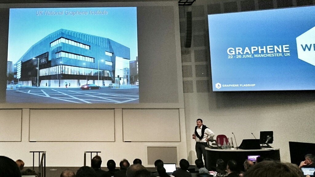
The UK welcomed an influx of graphene experts last week as Manchester University’s 200+ researchers working in the field of 2D materials were joined by hundreds more for Graphene Week 2015. The event, now in its 10th year, has grown from a small European workshop into a five-day conference boasting over 600 attendees and pushing the University Place venue to capacity. The scope of the programme has expanded too; hexagonal boron nitride (hBN), molybdenum disulphide (MoS2) and other related 2D materials have joined graphene on the ‘menu’ of structures being explored by developers. Most recently, the conference has been co-ordinated by the Graphene Flagship – a European drive to capitalize on the many opportunities for 2D materials, which launched in October 2013 and has adopted Graphene Week as its annual conference.
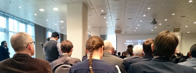
Plenary update: Nobel Prize winner Kostya Novoselov briefed the Graphene Week 2015 audience on major developments in the field of 2D materials.
The European Commission (EC) has given graphene and related 2D materials research a huge boost through its Flagship initiative, but as Thomas Skordas, head of the EC’s FET Flagships Unit, reminded the audience during the conference opening – the funding is not a blank cheque for 10 years. The objective is to deliver economic benefits. So far, Graphene Flagship projects have generated 3x more publications compared with the Horizon 2020 average, but to achieve its long term goal the programme needs to capitalize on this research growth.
Connecting with industry
The challenge of taking graphene and related 2D materials from the lab to the market is a focus issue for TMR+ and its sister journal Translational Materials Research (TMR), and we were delighted to be invited to the Flagship’s latest Graphene Connect workshop, co-located with Graphene Week 2015, to join in the discussion.
New facility: the Graphene Connect networking event focusing on investment opportunities was held at the UK’s National Graphene Institute in Manchester.
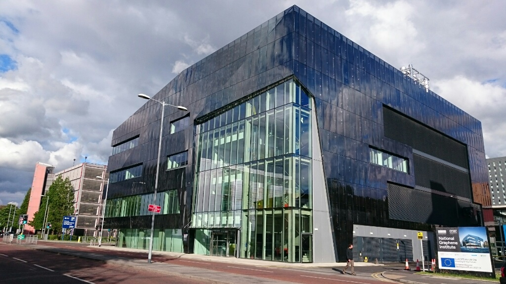
The Manchester session was focused on investment opportunities in graphene and related 2D materials, and put the spotlight on start-ups and early-stage companies. Fittingly, the workshop took place at the recently opened National Graphene Institute (NGI) – a facility where academia and industry are co-located to promote translation of 2D materials from the lab to the market.
Presenters from the VC community included Achim Hoffman of IP Group. He picked up on the issue of media hype surrounding graphene, which has distorted expectations. One of the key messages from the session was the need to stay focused on the fundamentals such as the market, the technology and the infrastructure. “You’ve got to go back to basics,” summed up MTI’s Mark Rahn, who also spoke at the event.
Rahn presented a snapshot of companies operating in the graphene sector. Today, materials suppliers are putting resource into stepping up the value chain by offering functionalized products and formulations that are easier for customers to evaluate and integrate. “The real hard work is how you get from a good idea to a viable production process,” said Nigel Salter, Managing Director of 2DTech – a start-up supplying graphene nanoplatelets (GNPs).
Other industrial players at the workshop included BGT Materials, a 2D materials venture with a base in the UK and a sister operation in Taiwan. According to its UK manager – Liam Britnell – BGT has developed an environmentally-friendly way to process graphene-oxide (GO). Applications include barrier films for food packaging, which exploits the material’s very low oxygen transmission characteristics.
Hexagonal highlights: the National Graphene Institute’s carbon-black coloured cladding is patterned with graphene-shaped perforations.
Whether it’s packaging or microelectronics, materials firms need to understand their potential markets and make sure that their products and processes are compatible with their target industries. To accelerate this process, Applied Nanolayers (ANL) – which grew out of Leiden University – decided to break the cord from academia early on and moved south to base itself in the heart of the Netherlands’ chip-making ecosystem. The company provides wafer-grown 2D material such as graphene or hBN for a range of device applications.
Business briefing
The final panel discussion of the day, which featured Graphenea, Haydale and Flexenable, highlighted the many different routes for growing and repositioning businesses in the advanced materials sector – topics that TMR will be exploring in more detail through its journal section ‘Policy, funding and business strategy’.
Graphenea began as a supplier of 2D materials for the research community, but the firm’s products also appeal to industry and in 2013 it won investment from Repsol – a multinational with activities upstream and downstream in the oil & gas sector. Most recently, Graphenea has been awarded Euro 2.5 million through the Horizon 2020 SME instrument – a phased programme of support to small-to-medium enterprises – which will allow the San Sebastian headquartered company to further scale-up its production capacity. The firm has a satellite office based in Boston, US, to strengthen its links with MIT and Harvard.
Haydale has raised capital by floating on the London Stock Exchange, and recently acquired EPL Composites, which gives the firm an immediate route into this applications area. Haydale has built a strong case for the benefits of graphene functionalization through independent testing of its materials by the UK’s national measurement institute – NPL.
FlexEnable was spun out of Plastic Logic to give the business more freedom to apply its expertise in printing transistors on plastic beyond the display sector. Its activities include consulting services to materials companies.
Meanwhile, back at Graphene Week
There was plenty of industry input at the main conference too with updates from Bosch, IBM and Alcatel Lucent, to name just a few of the big names eyeing up opportunities for 2D materials. TMR+ spoke with IBM’s Shu-Jen Han last year, and the message remains the same in 2015 – RF devices rather than digital logic are a stronger proposition for graphene. Telecomms could be a promising area for the material thanks to graphene’s consistent performance across a wide temperature range, and useful optical properties.
Smart space: The National Graphene Institute features a ‘high-rise wildflower meadow’ designed to improve roof function by providing a green space for people and pollinators such as bees, butterflies and hoverflies. For a video tour of the building, including the lab space, check out the YouTube clip from TMR+’s sister site physicsworld.com.
Alcatel Lucent has been working with partner AMO Aachen to investigate the potential of 2D materials in enabling highly-integrated photonic subsystems. The team has come up with a photodetector featuring CVD-grown graphene on a Si waveguide, which operates in the c-band (wavelength = 1550 nm) to support data rates up to 50 GBit/s.
The next Graphene Connect workshop is scheduled for early 2016 and will explore the topic of biosensors and implants. Graphene Week 2016 will take place in Poland next June.
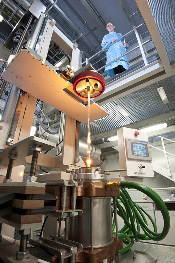
The University of Southampton’s Optoelectronics Research Centre (ORC) is making its next-generation optical fibre available for purchase. By broadening availability, the team aims to accelerate performance, differentiation, adoption and commercialization of optical fibre and photonics-based products.
Specialist optical fibre fabrication and coating. Image credit: University of Southampton
Designs include double-clad fibre for high average and peak power fibre lasers and amplifiers, and multi-element structures for space division multiplexed communication and sensing applications.
As part of the new service, the ORC will hold a number of research-grade fibres in stock for immediate delivery with the range continually adjusted over time to include cutting-edge designs. Fibres will be supplied for engineering development and research only. Once an application requires volume supply and the market demand is established, the ORC will work with commercial fibre manufacturers to transfer the fibre to production.
Translating research beyond the lab
The announcement gives developers early experience of working with ORC designs in order to evaluate structures from a market perspective and build a commercial case for future products.
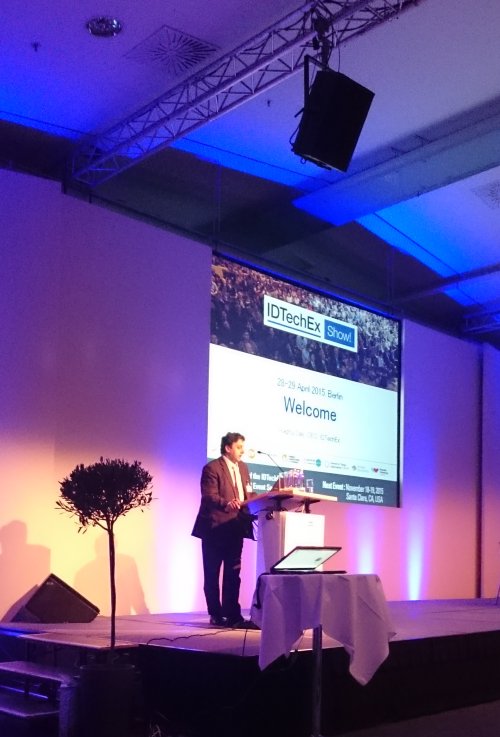
IDTechEx’s multi-track conference and exhibition explores the interconnected landscape of printed electronics, wearable technology, energy harvesting, the internet of things (IoT), graphene and 2D materials, 3D printing, and electric vehicles. Collaboration is key to succeeding in materials translation, and for me this was one of the big messages of the 2015 show, which brings together formulation specialists, systems developers, fabrication experts, measurement providers, and customer groups, all under the same roof for two days (or more if you sign-up to masterclasses).
Keynote welcome: Raghu Das, CEO of IDTechEx, briefs the audience on market projections for the printed electronics sector.
Dialogue between technology providers and end-users helps to resolve uncertainty in emerging fields such as printed and flexible electronics where – i) customers can be unsure about what’s possible and ii) suppliers need guidance on market requirements.
Bringing new technology to market
On day one, speakers from Qualcomm and Flextronics outlined how their firms bring new technology to the market. In Qualcomm’s case, its approach is built on four pillars – i) system R&D leadership, ii) design for manufacturability, iii) supply chain management and iv) customer support and engineering. It’s important not to overlook the final step. “The value proposition is only realized if you can propagate this to the customer,” Stein Lundby (R&D manager at Qualcomm) reiterated to audience.
Qualcomm, which Lundby describes as a ‘surface electronics’ company, is exploring opportunities for a hybrid product combining traditional crystalline based electronics with printed electronic components. Developed with Enfucell – a provider of printed power sources – the device features a 3-axis gyroscope and 3-axis accelerometer together with integrated battery and system electronics packaged in a band-aid style form factor. Users can stick the sensor on items such as golf clubs to determine how new products might improve their game, but this is just one possible scenario.
To navigate markets such as wearables, Flextronics – which focuses on production equipment and know-how – has opened design centres to help customers with product development and new use-cases such as electronic displays for athletic clothing. In his presentation, Keith Churches (head of innovation services at Flextronics) showed how the company brings new ideas to the market by configuring product-specific development networks that link the firm’s expertise with partners such as OEMs, universities and research institutes.
Nanomaterials Directa Plus – which was founded in 2005 and opened its graphene factory in 2014 – used the graphene and 2D materials conference track to talk through its collaboration with Vittoria Industries and highlight early market opportunities for graphene. Dubbed the wonder material, graphene – an ultra-thin layer of carbon – has been shown to have record-breaking electrical, thermal and mechanical properties, but breakthrough results in the lab don’t guarantee commercial success. “You have to be brave to be in the graphene market,” Giulio Cesareo (CEO of Directa Plus) commented.
Full house: interest in graphene and related 2D materials remains strong.
Vittoria uses Directa Plus’ graphene nanoplatelets to formulate bicycle tyres and wheels with enhanced properties such as heat dissipation and lateral stiffness. There are 165 wheel makers in the world, Rudi Campagne (founder of Vittoria Industries) told the audience, and the use of nanomaterials such as graphene is an effective way for Vittoria to differentiate itself from the competition.
Early uses of graphene provide a platform for growth in other sectors by establishing a materials supply chain. Beyond tyres and wheels, Directa Plus is looking at opportunities for graphene in cleaning up contaminated soil and water. In his talk, Cesareo explained that linked graphene platelets have the potential to remove hydrocarbon pollution from lakes, according to test results. Literature from the firm claims that 1 gram of its Graphene Plus sorbent can adsorb up to 80-90 grams of oil – for more details, visit the GEnIuS project website, a programme co-founded by European Union within the Eco-Innovation initiative.
Exhibition: new products launched at the show included Ceradrop’s ‘F-Serie’ multi-material printer.
The discussion then moved on to opportunities for 2D materials in the electronics industry. If graphene does make an impact in this sector it is likely to be driven by novel applications, based on the views of the speakers in the opening session. “Graphene will not replace silicon in standard devices,” commented Guenther Ruhl (lead principal in new materials at Infineon Technologies) during his talk.
Touch screens are also looking unlikely as a big opportunity for graphene. “Graphene transparent conductive films are among the worst performers in a crowded market,” explained Khasha Ghaffarzadeh (head of consulting at IDTechEx). Like Ruhl, he feels that 2D materials could have more impact in new product categories. “The beauty of graphene is that there are many target industries and applications,” Ghaffarzadeh added.
OPV and R2R technology
Analyst events such as the IDTechEx show give attendees a view on tomorrow’s technology today. Two further highlights for me from the keynote presentations were Heliatek’s building integrated photovoltaics (BIPV) and Asahi Kasei’s e-beam fabricated seamless roller for printing transistors.
Show venue: Estrel, Berlin
In the afternoon on day one, Martin Pfeiffer (chief technology officer at Heliatek) outlined what he feels is a sweet spot for OPV – active facades. To compete with silicon, OPV has to bring something different, which it can when applications demand flexible and lightweight solutions. He added that the energy payback for an OPV cell can be as little as 3 months, as determined by the EU project dubbed X10D. Pfeiffer revealed that large-scale trials of the firm’s material were now underway in China and Germany on concrete (in Shanghai), PVC membrane (in Berlin) and glass (in Dresden) structures, with another pilot project due to start soon in Singapore on a glass and steel construction.
There were more glimpses of the future on day two when Masayuki Abe of Japanese giant Asahi Kasei – which operates in chemicals, electronics and healthcare sectors – presented his team’s work on seamless roller mold (SRM) technology for roll-to-roll (R2R) printing of sub-micron feature sizes. To make the mold, they rotated a super-smooth (2 nm roughness) roller under an e-beam writer. Moving the roller laterally (as well as rotating it) allows the team to create complex mold patterns. To test the process, Abe’s group used one of its roller molds to print a 200 ppi, 125 micron pitch TFT array. Abe was clearly proud of his team’s results and sees a bright future for the technique. “SRM will bring about the realization of high-resolution printing,” he told the audience.
Dates for your diary
The IDTechEx conference and exhibition takes place twice annually – once in Europe and once in the US (18-19 Nov 2015). The event returns to Berlin on the 27th and 28th of April 2016.
Europe’s Graphene Flagship has released details of its 6th Graphene Connect workshop, which aims to introduce business angels to graphene and create an arena for small to medium enterprises (SMEs) and venture capital (VC) firms to interact.
‘The purpose of the flagship is not to perform research — it’s to bring research into society,’ Helena Theander, a senior member of the Graphene Flagship’s innovation team, told Translational Materials Research (TMR) in a recent article highlighting the need to engage SMEs in materials commercialization. ‘Graphene Connect is a process to get more industry players interested in graphene and related 2D materials.’
This latest installment in the Graphene Connect series coincides with Graphene Week 2015 and will take place in Manchester, UK, on Monday 22 June.
The workshop programme includes –
Presentations by firms operating in the graphene sector.
VC talks on investing in graphene given by industry representatives, followed by a panel discussion.
Matchmaking activities for SMEs and entrepreneurs to meet and interact with the venture capital community and explore business opportunities.
To register for the workshop, visit the event website.
There’s plenty of talk about the hurdles that scientists have to overcome to commercialize their research, and while there’s nothing wrong in recognizing the scale of the challenge, it’s important to celebrate the success stories too. The Royal Society strikes a positive note in its recent video featuring Nanoco, Solexa and ARM, which offers advice on translating technology from the lab to the market.
Winning investment
The speakers are well placed to comment on the journey from discovery to devices, and each of them discusses different pieces of the puzzle, which includes raising money.
In the clip, Paul O’Brien, a professor at the University of Manchester and co-founder of Nanoco, emphasizes that the trickiest part to get funded is the step between invention and product development. To grab the attention of potential backers, it helps to think like one.
“The pull for the investor is the potential for a market,” O’Brien explains in the video. “So, if you can point towards a market like displays and say that [your product] could be in every house, in every country in the world, then they start to look interested.”
– You can find more videos from the Royal Society on its YouTube page
For additional case studies, check out the following articles from the journal Translational Materials Research –
Access to venture capital is frequently identified as a key factor in moving ideas beyond the lab and enabling start-ups to turn functional prototypes into market-ready devices.
“Venture capital can bring not just money to a project, but also business skills and technical knowledge, which are different from the connections and advice that the state and the region can provide,” Serdar Sariciftci, a leading researcher in the field of organic photovoltaics, told Translational Materials Research (TMR) in a recent interview. “Experienced venture capitalists (VCs) who have done this thing before in similar sectors are invaluable to a scientist like me.”
VCs are well-placed to examine what it takes to translate research breakthroughs into products and TMR is fortunate in being able to draw upon the experience of Andrew Haughian, partner at Pangaea Ventures and a member of the journal’s Editorial Board. Haughian is a regular contributor to TMR, and has written for the journal on the topics of ‘Focus’, ‘Licensing’ and ‘Funding mathematics’, with more articles in the pipeline.
Here are 10 tips from the discussion so far, with links to the original opinion pieces after the bullet points.
Highlights from the VC desk
On the one hand, there is a temptation to ‘add value’ by demonstrating as many applications as possible. On the other, there is the repeated message to do one thing and do it well. The reality is that the key to building an important and valuable company usually lies somewhere in between.
The 80:20 rule applies to start-ups. 80% of the effort is focused on getting the first product to market, while 20% is spent on what’s next. The first product should meet minimum market requirements, and market entry should primarily facilitate organizational learning about the market and operations while at the same time building a brand.
An ideal licensing situation is when there are levers in addition to intellectual property (IP) that can be incorporated into the licensing negotiation. One lever is the control of a key ingredient(s) used in the production process.
Getting technology into the market as soon as possible is critically important, while the real game-changer continues to brew. The key here is that the next-generation technology must be substantially differentiated in terms of IP and product benefits, such that a ‘Gen One’ licensee does not effectively undermine the possibility of successfully commercializing ‘Gen Two’.
There are many considerations in picking the best licensee partner(s), but picking a brand name that will lend credibility should be at the top of the list.
A licensing deal can create a significant draw on management and technical resources, so care must be taken to ensure core activities are not disrupted.
When mergers and acquisitions is the likely endgame, acquirers are unlikely to pay a technology premium unless they truly believe that buying a company gives them a long-term sustainable advantage.
In many cases, new materials technologies are competing against incumbent commodity-like products. Usually these incumbent technologies are well along in bottoming on the cost reduction curve, whereas the new technology is starting at the top.
Poor consideration of value chain issues usually ends up being the Achilles’ heel of even the most exciting materials technologies. Finding the right set of partners that complement the core value proposition is vital for eliminating the cost and time of reinventing the wheel.
There are a lot of moving parts in getting focus right. The good news is that this critical commercialization skill is transferable to other technology industries, and so a vast network of management talent can be tapped.
Original articles from the journal Translational Materials Research (TMR)
In the latest physicsworld.com podcast, Josh Silver – a physicist and inventor based in Oxford, UK – introduces his liquid lens enabled adjustable eye-wear. Dubbed Adspecs, the product offers an alternative eye-care model by allowing wearers to tune the power of their spectacles. To do this, users put on the glasses and pump fluid into lens chambers formed between clear, high optical quality plastic films, which changes the curvature of these flexible structures and brings the wearer’s view of the world into focus. To complete the simple setup procedure, the left and right eye adjusters are locked-off leaving the spectacles fixed at the correct prescription.
Physicist and inventor Joshua Silver of The Centre for Vision in the Developing World talks to physicsworld.com about the prospects for self-adjustable glasses.
In the interview, Silver talks about the positive impact his invention could have in regions such as sub-Saharan Africa where there are insufficient numbers of optometrists to deliver vision correction through the conventional approach of eye-tests and traditional glasses. He also describes the challenges of taking his ideas from the lab and bringing them to mass market. Silver came up with his first prototypes in 1985 and through the work of The Centre for Vision in the Developing World he hopes to see a billion people having Adspecs-enabled vision correction by the year 2020.
Barriers to success
It’s easy to pinpoint cost and performance as important considerations, but as Silver explains, there were other lessons to be learnt when translating the technology from first prototypes into products with market appeal. “When people meet one another, they tend to look at their eyes,” he commented. “People are very sensitive about what their eyes look like and so you’ve got to get the fashion right as well as the optical function.”
Europe’s Graphene Flagship – a € 1 billion research initiative tasked with bringing together academia and industry to translate 2D materials from the lab to the market – has released an Open Access version of its science and technology roadmap highlighting key application areas for graphene and related structures and providing estimates of timelines to market.
The report (PDF | Rich HTML) includes the views of more than 60 academics and industrial partners, and concludes a four-year project to collect and coordinate information “to guide the community
towards the development of products based on graphene, related two dimensional (2d) crystals and hybrid systems.”
The roadmap flags flexible electronics, composites, and energy as three areas that could generate close-to-market products within a 10-year timeline. Further out, the programme hopes to see silicon-integrated photonic devices, sensors, high-speed electronics, and biomedical devices based on 2D materials also making an impact beyond the lab.
Supercapacitors are a promising application for advanced materials such as high surface area nanocarbons, but what are the translational issues and market factors that researchers need to consider to win-over commercial partners? To find out more on the topic, TMR+ spoke with Franco Gonzalez, a senior analyst at IDTechEx and co-author of ‘Electrochemical Double Layer Capacitors: Supercapacitors 2014-2024’ – a 10 year forecast analysing the market, applications, technology, patent and profit trends, and key players in the sector.
Advantages over batteries
Supercapacitors don’t rely on chemical reactions and this gives them several advantages over batteries including a higher power capacity per unit mass, superior operation at low temperatures and extended operational lifetime. Truck-makers are using supercapacitors to guarantee that vehicles will start in very cold weather – a scenario where lead-acid batteries perform poorly as their energy capacity can be reduced by as much as 50%.
The longer cycle lifetimes of supercapacitors compared with batteries can lower system maintenance costs and improve reliability. It makes devices attractive for large resource power applications, particular in remote locations. In wind farms, supercapacitors are used to power actuators that change the blade pitch in high winds to protect the turbines.
IDTechEx senior analyst, Franco Gonzalez
Energy recovery
Although supercapacitors store less energy than batteries, they can be charged very quickly without detriment (unlike batteries). This makes them ideal for regenerative breaking systems, for example on trains and trams, which convert kinetic energy into electricity. They can also be configured to recover potential energy stored in cranes operating at cargo loading and unloading sites. “At ports, these machines can be in use almost constantly, so it’s a great opportunity for energy recovery,” said Gonzalez. “The need to reduce CO2 emissions is driving the market.”
It often makes sense to pair a supercapacitor and a battery together. “Power surges reduce the energy capacity of a battery,” he explained. “But you can protect it using a supercapacitor.” The combination can be used to extend the lifetime of batteries in renewable energy systems, or in smart phones where power-demand fluctuates depending on the functions in use.
Industry factors
As a general rule, supercapacitors are well-suited to applications with highly-variable power demands. In principle, this means they are a great match for ‘stop-start’ systems fitted to modern cars, which switch-off the engine while you are waiting in traffic or at stop lights and then restart the vehicle when you engage the gearbox. Unfortunately, it’s not that simple.
“Different industries focus on different parameters,” Gonzalez cautioned. “Auto-makers are looking for supercapacitors that are half the price of current devices as they focus on the cost per unit energy and are concerned about the selling price of the car.”
Sales of electric buses and on the other hand are much less sensitive to the initial purchase price as buyers in this sector pay more attention to the total cost of ownership of the vehicle. In this case, because supercapacitors bring down the price per charging cycle, the market is more lucrative for developers.
Today, supercapacitors are more attractive to industrial users that are open to considering the system level cost rather than the cost per unit energy of devices. But, as Gonzalez points out, supercapacitor manufacturers are nevertheless working hard at the material level to reduce price and improve device performance to offer a better cost per unit energy to customers.
Device development
Advances in materials can contribute in a number of ways to making supercapacitors more competitive in the market. Increasing the surface area of the electrodes through activated carbons and nanomaterials will drive up the capacitance and benefit the energy storage capacity of the device. At the same time, finding ways to reduce the resistance (of the active material, the electrolyte, and the porous separator) will boost the power output.
However, it is the operation of supercapacitor cells at higher voltages (V) and finding the right materials to make this happen, which may impact performance in the short to medium term. Both the power and the energy of a capacitor are proportional to V2. “Electrolytes in organic solvents can withstand 2.7 V, but developers are also looking at ionic liquids – room temperature salts – that operate at 5V,” said Gonzalez.
Devices come in many shapes and sizes, and he highlights micro-supercapacitors as a particularly exciting and growing area of research. Gonzalez advises researchers to look at lower-cost materials and manufacturing methods in the first instance. “If you want to use expensive materials then you need to find an application that will pay for that,” he commented. “Researchers need to be aware of how the industry is changing and the relative sensitivity to price of the different applications.”