Olympus has released an application note showing how optical metrology can be applied to improve the lifetime and performance of flexible electronics.
The study highlights the work of Dario Gastaldi and his team at the Politecnico di Milano, Italy, who have used laser confocal scanning microscopy to demonstrate how particular interconnect geometries are more resistant to delamination.
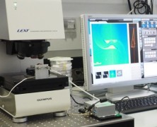
Optimizing interconnect design: micro-tensile testing device coupled to a laser confocal scanning microscope
The group’s apparatus features an in-situ micro-tensile testing device coupled to high-resolution imaging equipment (Olympus LEXT OLS4100) and allows the researchers to examine the two main features that have been found to affect adhesion between the interconnect and polymer substrate: geometric parameters and the fabrication process itself.
Design tool
Observing the interconnects under mechanical testing allows the team to focus on key parameters such as strut length and obtain quantitative information, which can be fed back into the design cycle. 3D optical profiles of interconnect geometries allow developers to monitor samples for signs of surface cracking, which can be used to optimize manufacturing processes.
In the work, the researchers observe that plasma treatment of polymers, while increasing adhesion, may promote cracking.
Related links
– Lab to market highlights: TMR anniversary collection (free to read)
– Flexible and Printed Electronics – a new journal from IOP Publishing
vtmlhjr